기사입력 2024.08.21 15:01
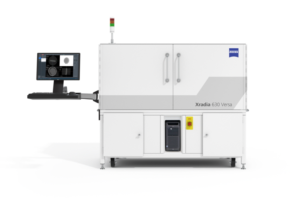
자이스는2.5/3D 및 팬아웃 웨이퍼 레벨 패키지 등 첨단 반도체 패키지의 불량분석을 위한 고해상 3D 엑스레이 이미지 처리 솔루션 3종을 발표했다. 서브 마이크론 및 나노 패키지 FA 작업에 사용되는 세 가지 신제품은 엑스레디아 600 시리즈 버사, 엑스레디아 800 울트라 엑스레이 현미경, 그리고 새로운 엑스레디아 콘텍스트 마이크로CT다. 자이스는 기존 제품군에 이 제품들을 추가함으로써 반도체 업계를 위한 방대한 3D 엑스레이 이미지 처리 기술 포트폴리오를 제공하게 됐다.
2019-01-23 오후 5:01:03by 이수민 기자
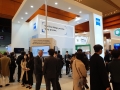
글로벌 반도체 산업 전시회인 ‘세미콘 코리아 2023’가 코앞으로 다가왔다. 매년 반도체 산업의 성장과 최신 반도체 제조 기술을 확인할 수 있는 이번 자리에 EUV 장비에 핵심이 되는 소재 기업 ZEISS 코리아도 참여해 선진 기술력을 선보일 예정이다.
2023-02-01 오전 11:42:52by 권신혁 기자
반도체 소재 부문의 강자인 독일 기업 자이스 코리아(ZEISS, 대표이사 정현석)가 오는 1월31일부터 2월2일까지 서울 코엑스에서 열리는 ‘세미콘 코리아 2024’에 참가한다.
2024-01-18 오전 11:38:24by 배종인 기자
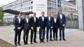
이재용 삼성전자 회장이 독일 오버코헨 자이스(ZEISS) 본사를 방문하고, 부품, 장비 등을 살펴보며 자이스와 반도체 협력 강화가 급물살을 탈 것으로 전망된다.
2024-04-29 오후 3:47:49by 배종인 기자

[열린보도원칙] 당 매체는 독자와 취재원 등 뉴스이용자의 권리 보장을 위해 반론이나 정정보도, 추후보도를 요청할 수 있는 창구를 열어두고 있음을 알려드립니다.
고충처리인 장은성 070-4699-5321 , news@e4ds.com


