


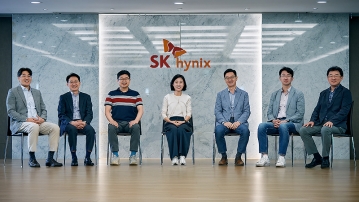
“AI and device convergence drives changes in the semiconductor market”… Expected memory demand from the metaverse
Demand for high-performance, high-bandwidth semiconductors supporting AI learning and inference is rapidly increasing. In particular, with the DRAM ma…
2024.05.30 by 권신혁 기자
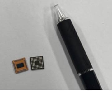
Nepes to commercialize AI semiconductor packaging technology
Netpass has completed the development of PoP technology, which is a foundational technology for 2.5D packaging, utilizing its proprietary redistributi…
2024.05.20 by 배종인 기자
Japanese semiconductor post-processing to be distributed to Japan
Japanese semiconductor equipment and material companies are joining forces with Intel to undertake full-scale technology development for semiconductor…
2024.05.17 by 배종인 기자

SK Hynix, TSMC join hands...Strategic collaboration on HBM4 packaging
SK Hynix, which holds market leadership in HBM technology, is expected to move into mass production of customer products for next-generation HBM4 by l…
2024.04.19 by 권신혁 기자

SK Hynix Vice President Woojin Choi: “We will strengthen our advanced packaging technology leadership through limitless challenges”
SK Hynix's P&T (Packaging & Test) head Vice President Choi Woo-jin has dedicated himself to research and development in memory semiconductor packaging…
2024.04.12 by 권신혁 기자

SK Hynix Invests 5.2 Trillion Won in AI Advanced Packaging
SK Hynix has decided to construct an advanced packaging production facility for AI memory in West Lafayette, Indiana, USA, and to collaborate with loc…
2024.04.04 by 배종인 기자
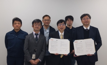
Korea Packaging Industry Association, Japan Join Hands to Develop Advanced Packaging Super-Gap Technology
The Korea Printed Circuit Board Industry Association (KPIA, Chairman Kim Hyun-ho, headquartered in Cheongju, North Chungcheong Province) has concluded…
2024.02.29 by 배종인 기자
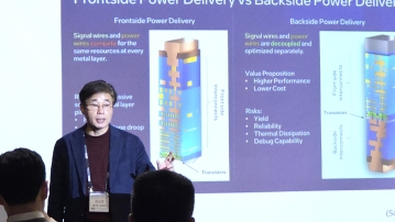

“'Hybrid Bonding' is the Trend, Particle Management is Key”
"Packaging technology is shifting from post-process to pre-process. The paradigm has changed. Accordingly, semiconductor equipment and materials compa…
2024.02.26 by 권신혁 기자
Nepes begins mass production of advanced PMIC packaging
Semiconductor backend processing company Nepes has recently begun receiving orders for power semiconductors for artificial intelligence (AI) chipsets …
2024.02.26 by 배종인 기자
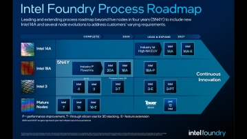
Intel Launches Systems Foundry...1nm Shipments in 2025
The advanced semiconductor foundry market is prepared to expand from a two-way competition into a three-way battle. Intel has launched a full-fledged …
2024.02.22 by 권신혁 기자
Investing 39.4 billion won to secure semiconductor packaging strategy technology
The Ministry of Trade, Industry and Energy (Minister Ahn Deok-geun) will announce the "Electronic Components Industry Technology Development (Advanced…
2024.02.13 by 배종인 기자
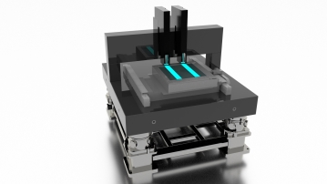
Applied Materials, Ushio Collaborate to Launch Digital Lithography
As AI workloads increase rapidly, demand for semiconductor chips with superior capabilities is growing. As AI miniaturization requirements exceed what…
2024.01.04 by 권신혁 기자
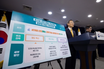
Securing ultra-gap source technology, supporting advanced packaging and on-silicon displays
In the Year of the Wood Dragon, support for securing next-generation foundational technologies in the three strategic fields of semiconductors, displa…
2024.01.02 by 권신혁 기자

Intel Announces Next-Generation Transistor Scaling Technology
A 3D stacked CMOS transistor employing 'backside power delivery technology' and 'backside direct contact' has emerged.
2023.12.11 by 명세환 기자
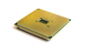
We listened to feedback from the field to ensure the success of our 100 billion won investment in semiconductor packaging over five years.
Minister Lee Jong-ho of the Ministry of Science and ICT visited the research site at LG Innotek regarding substrates for advanced semiconductor packag…
2023.12.05 by 배종인 기자