

SK Hynix, 3Q23 Performance Cold Wave Continues...DRAM Turns to Profit
SK Hynix held an earnings presentation on the 26th and announced that it posted negative operating profit and net loss in the third quarter of this ye…
2023.10.27 by 명세환 기자
BSM between vehicles to be mandatory by 2026… EMC perspective required
The mobility sector is experiencing rapid transformation driven by environmental sustainability and electrification trends. Consequently, traditional …
2023.10.23 by 명세환 기자
Ansys Supplies 'Thermal and Power Integrity Solution' to Samsung Foundry
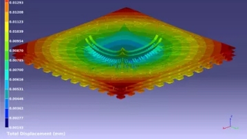
Ansys Korea, a global leader in engineering simulation software (CEO Moon Seok-hwan), is closely collaborating on power and thermal management for adv…
2023.10.23 by 배종인 기자

Schott Strengthens Advanced Packaging Glass Substrate Portfolio for the AI Era
Global specialty glass leader SCHOTT is now actively undertaking product development, optimization, and investment initiatives to address the growing …
2023.10.19 by 배종인 기자
Intel Unveils Next-Generation Packaging 'Glass Substrate' Technology
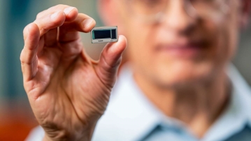
The semiconductor industry is seeking answers in next-generation advanced packaging to achieve Moore's Law. Intel has found a clue in 'glass' material…
2023.09.19 by 명세환 기자
A place where electromagnetic waves, packaging, and artificial intelligence technologies converge
Electrical design based on electromagnetic engineering is a critical element in system semiconductor development in advanced packaging processes where…
2023.09.04 by 명세환 기자
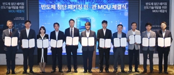
Semiconductor Advanced Packaging, Public-Private Partnership
The Ministry of Trade, Industry and Energy, Samsung Electronics, SK Hynix, LG Chem, Hana Micron, Protec, Sapion Korea, Simtec, the Next-Generation Int…
2023.08.29 by 배종인 기자
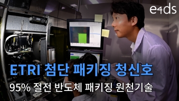
ETRI, Development of 95% Energy-saving Semiconductor Packaging Source Technology
The Electronics and Telecommunications Research Institute (ETRI) has developed an advanced semiconductor chiplet packaging technology that reduces pow…
2023.07.28 by 배종인 기자


EMI/EMC(1)-EMI packaging, increasing demand in mobile and automotive
"Packaging is not a single major field. Semiconductor packaging contains everything—electronics, mechanics, materials, and chemistry all mixed togethe…
2023.07.20 by 명세환 기자
Applied, Hybrid Bonding·TSV New Technology Launched… Heterojunction Chip PPACt Improvement
Heterogeneous Integration (HI) is an advanced solution that increases performance and density while reducing costs. As semiconductor manufacturing app…
2023.07.18 by 명세환 기자
Cadence Supports Samsung Foundry's Development of Advanced Packaging Technology
With growing interest and demand for advanced packaging for heterogeneous integration, Cadence, a global semiconductor design automation company, and …
2023.07.06 by 명세환 기자
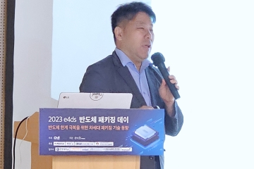
Semiconductor Market Recovery Remains Question Mark This Year… Focus on AI Semiconductors
At the 2023 e4ds Semiconductor Packaging Day, there were forecasts suggesting that the semiconductor market this year may not recover easily.
2023.07.03 by 명세환 기자

Fabier Shu, Senior Manager, Applied Semiconductor Packaging Success Strategies
Favier Shoo, Senior Manager of Strategic Marketing for the Packaging Business Division at Applied Materials and a global expert in semiconductor packa…
2023.06.12 by 배종인 기자
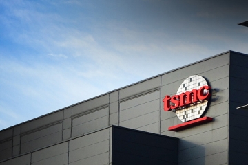
TSMC Opens 6 Advanced Back-end Fabs for Advanced Packaging and Testing
TSMC has begun operations at a new backend fab facility for advanced packaging and testing, moving to improve advanced semiconductor production yield …
2023.06.09 by 배종인 기자
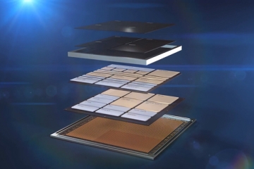
'Semiconductor Packaging' Left Behind While Claiming to Become a Semiconductor Superpower
While the government proclaims the achievement of semiconductor superpower status in the domestic industry, voices are growing louder calling for conc…
2023.06.08 by 배종인 기자