AI, IoT, 블록체인, RADAR, 5G, 8K 비디오 등의 발달로 메모리 처리량이 급증하고 있다. 그러나 기존의 메모리 대역폭은 시스템 요구사항의 증가를 따라가지 못하고 있다. 업계에서는 이에 TSV 기술을 활용한 HBM2 DRAM을 통해 대용량 메모리 솔루션을 모색하고 있다.
메모리 대역폭 증가의 한계
HMC, HBM2 등으로 극복
저전력, 소형화 추세 충족
시스템 요구사항의 폭발적 증가
지난 수년간 메모리 대역폭과 시스템 요구사항은 비례적으로 증가했다. 그러나 최근 AI, IoT, 블록체인, RADAR, 5G, 8K 비디오 등의 발달로 산업전반에서 요구하는 메모리 처리량이 급증한 반면, 메모리 대역폭의 증가는 이를 따라가지 못하고 있다.
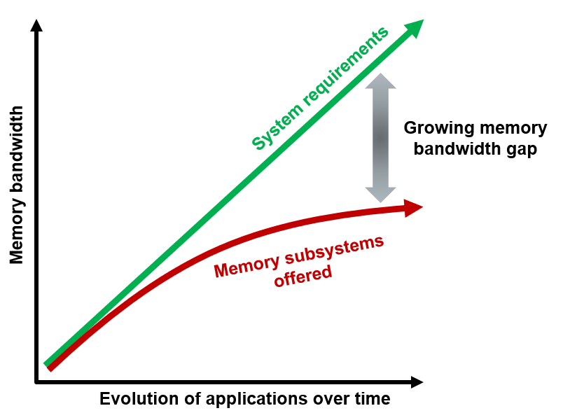 메모리 대역폭의 증가세가 둔화되고 있다
현재 가장 많이 쓰이는 DDR 메모리의 대역폭은 지난 20년동안 세대가 올라 갈 때마다 2배씩 증가했다. 그러나 DDR5의 상용화는 아직 요원하고 2배씩 증가하는 것만으로는 최근의 추세를 따라가기 힘들다.
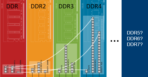
DDR5 메모리의 출시는 2019년으로 예상된다
메모리 대역폭의 한계는 입출력의 제한 때문에 발생한다. 그러나 더 많은 컴포넌트를 사용하는 건 대안이 될 수 없다. 컴포넌트가 많아지면 병렬 신호 트랜스가 발생한다. 이 신호를 고속으로 처리하기 위해 버퍼를 추가하면 시스템이 제공하는 전력 용량 범위를 초과할 것이고 공간도 차지한다.
컴퓨팅 기기에 메모리를 직접 통합하는 방법이 있다. FPGA 또한 메모리 블록을 포함하고 있기 때문이다. 그러나 전문화된 특성을 갖고 있어 충분한 양을 제공하진 못한다. 표준 고용량 메모리 기술을 FPGA에 직접 통합할 수는 있지만 용량에 한계가 있다. 따라서 높아져만 가는 시스템 요구사항을 만족하기 위해서는 기존의 보편적인 메모리 하드웨어 구조를 타파하는 새로운 기술 혁신이 필요하다.
저전력 소형화 추세에서 메모리 대역폭 늘리기
업계에서는 DDR3/4보다 3D 적층 메모리에 집중하고 있다. 3D 적층 메모리는 작은 폼 팩터에서 대용량 구현이 가능하기 때문이다. 3D 적층 메모리를 사용하는 방식은 두 가지다.
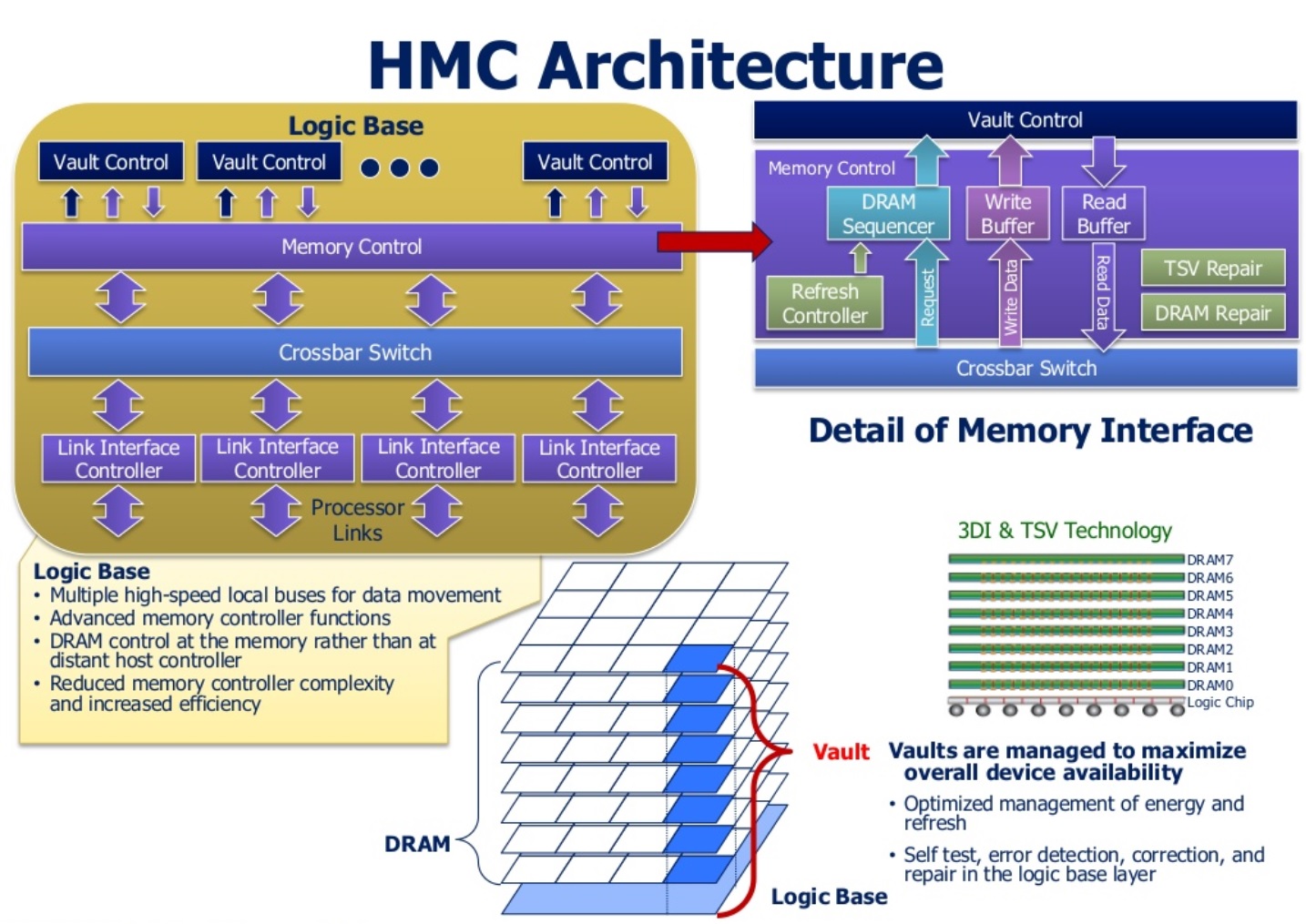
마이크론의 HMC 아키텍처
2011년에 개발된 마이크론의 HMC(Hybrid Memory Cube)다. 3D TSV(Through Silicon Via, 실리콘 관통전극) DRAM 적층 기술을 사용하여 최대 320GB/s까지 동작한다. 적층 된 메모리는 컴포넌트 내의 컨트롤러를 포함한 베이스 다이와 연결된다. 보드에 별도의 기기로 구성되어 역시 별도의 파워 및 터미네이션 회로가 필요하고 전력 소모가 상대적으로 많다.
.jpg)
AMD와 SK 하이닉스의 1세대 HBM
2013년에 개발된 AMD와 SK 하이닉스의 HBM(High Bandwidth Memory)은 메모리층을 TSV 기술을 사용하여 연결하는 방식은 HMC와 동일하다. 병렬 인터페이스를 채택했으며 병렬 버스를 사용하여 높은 대역폭 구현이 가능하다. 또한, 컴퓨팅 제품 내부에 집적되어 보드에서의 긴 트레이스를 피한다.
HBM2의 빛
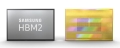
삼성전자와 SK 하이닉스가 2016년 8월에 발표한 HBM2은 그해 10월 JEDEC(Joint Electron Device Engineering Council)에서 표준으로 채택한 2세대 HBM 규격이다. HBM2 적층은 256GB/s까지 동작하며 4층까지 쌓으면 최대 1GHz까지 동작한다. 외부 메모리처럼 사용할 수 있어 1024Bit 병렬 인터페이스를 가지고 있다. 그리고 HMC와 달리 베이스 다이에 컨트롤러를 포함하지 않는다. 컨트롤러는 호스트 기기에 구성되어 있다. HBM2를 사용하기 위해서는 대용량의 병렬 데이터를 칩 내에서 연결하는 기술이 필요하다.
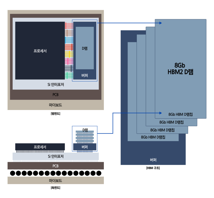
삼성전자의 HBM2 DRAM 구성 사례
전통적인 DRAM은 PCB 트레이스로 연결한다. 반면 HBM2는 패키지 내 on-die 방식으로 연결한다. HBM2는 작은 풋프린트를 가지고 있으며 기존 DRAM에 비해 전력 소모가 적다. 그리고 PCB 트레이스와 외부 터미네이션 저항이 필요 없다.
e4ds의 9월 13일 ‘인텔 FPGA 를 사용한 대용량 대역폭 메모리 솔루션’ 웨비나에서는 메모리 대역폭이 직면한 한계를 짚어보고 HBM의 특징을 알아본다. 그리고 HBM을 집적한 인텔의 FPGA를 중심으로 HBM의 컨트롤러를 용도에 맞게 최적화하는 방법 또한 다룰 예정이다.
알파고의 충격이 엊그제 같건만 어느새 AI와 IoT가 우리 일상에 깊게 파고들었다. 자동차 업계에서는 2025년, 무인 자동차의 상용화를 점치고 있다. 데이터 분석 기술의 발달이 가져온 진보다. 그만큼 디바이스와 데이터 센터가 처리해야 할 데이터양이 기하급수적으로 증가하고 있다. 기존의 DDR램을 뛰어넘는 메모리 대역폭을 지닌 HBM2가 가져올 미래가 궁금한 이유다.