2010년대부터 반도체 공정 미세화 난도 증가로 반도체 칩 성능의 향상이 더뎌지며 무어의 법칙에 대한 의문이 제기되고 있다. 그러나 EUV 공정이 본격적으로 도입되며 무어의 법칙이 다시금 연장될 것으로 예상된다. EUV의 파장은 13.5nm로, 기존부터 널리 활용되는 ArF의 193nm보다 훨씬 짧아 반도체 노광 공정의 정밀도를 높일 수 있다.
ArF보다 파장 짧은 EUV, 반도체 공정 미세화
EUV 공정, 전력원 필요하고 금속 오염 심해
5nm 이하에서 DPT/QPT 공정과 병행 사용
무어의 법칙은 반도체 칩 성능이 18개월마다 2배씩 증가한다는 법칙이다. 인텔의 공동창립자인 고든 무어(Gordon Moore)가 1965년 주장한 이 법칙을 바탕으로 반도체 업체들은 그간 제조 전략을 세워왔다.
하지만 2010년대부터 공정 미세화 난도 증가로 반도체 칩 성능의 향상이 더뎌지며 무어의 법칙에 대한 많은 의문이 제기되고 있다. 그러나 반도체 공정에 극자외선(Extreme Ultra Violet; EUV) 공정이 본격적으로 도입되며 무어의 법칙이 연장될 것으로 예상된다.
한국반도체산업협회(KSIA)에 따르면, EUV의 파장은 13.5nm로, 기존부터 널리 활용되는 불화아르곤(ArF)의 193nm보다 훨씬 짧아 반도체 노광 공정의 정밀도를 높일 수 있다.
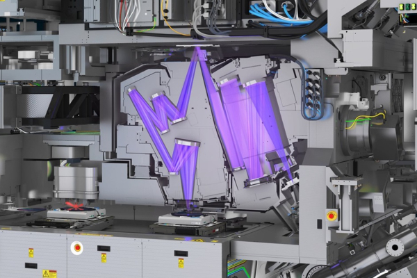
▲ EUV 장비 내부 [그림=ASML]
차세대 반도체 미세공정을 실현하는 방법으로 주목받는 EUV 공정은 현재 로직, 파운드리 공정을 중심으로 적용이 이뤄지고 있다. 두 분야의 경우 7nm 이하에서는 DPT(Double Patterning Technology)/QPT(Quadruple Patterning Technology) 공정보다 EUV 공정을 활용하는 게 비용 측면에서 이득이다.
하지만 EUV 기술만을 사용하여 원가 경쟁력을 갖추기보다는 미세공정 일부를 EUV 기술이 담당하는 방향으로 전개될 것으로 업계에선 예상한다. EUV는 전력원을 위해 별도의 발전소가 필요할 정도로 구현 난도가 매우 높고 금속오염(Metal Contamination)도 심하다.
현재 업계는 미세한 패턴을 구현하기 위해 대부분 기존 ArF 액침(Immersion) 장비를 사용한다. ArF 액침은 이론상 40nm 공정까지 사용할 수 있다. 30nm 공정 이하에서는 ArF 액침 장비에 DPT 공정을 추가로 사용하는 상황이다.
EUV를 이용하면 노광 공정을 반복하지 않고도 7nm 및 5nm 공정 구현이 가능하다. 문제는 양산성이다. 따라서 미세패턴이 필요한 부분에는 국부적으로 EUV를 사용하고, 다른 부분에는 기존 액침 공정을 사용하는 방향으로 기술이 개발될 것으로 판단된다.
또한, EUV로 5nm 이하 공정을 구현해야 한다면, EUV에 DPT 공정을 도입해야 하는 문제가 발생한다. 따라서 5nm 공정 이하에서는 EUV와 함께 DPT, QPT 공정을 함께 활용해야 할 것으로 보인다.
향후 노광 공정은 하나의 기술을 적용하기보다는 다양한 기술을 접목하는 쪽으로 개발될 것으로 판단된다. EUV 기술과 기존 노광 반복 공정인 DPT, QPT 및 대체기술 개발을 통한 공정 미세화가 지속될 전망이다.
◇ EUV 도입으로 반도체 구조와 소재도 변화할 것
로직과 파운드리 분야에선 7nm 이후 EUV 도입이 진행 중이며, 3차원 구조도 병행해서 기술 개발이 진행되고 있다.
5nm 혹은 4nm 공정까지는 EUV를 단독 사용하지만, 5nm 이하에서는 EUV 기술에 DPT나 QPT 기술을 적용하고, 구조 역시 FinFET을 뛰어넘는 GAA(Gate-All-Around) 방식으로 변화가 예상된다.
DRAM 분야에선 1zm 이후 EUV 기술도입이 본격화되며 캡(Cap) 공정에 산화하프늄(HfO2) 등 소재 기술의 다변화가 예상된다.