[편집자주] 반도체 업계 낸드플래시 적층이 200단을 넘어섰다. 싱글 스택으로 128단을 쌓은 삼성전자 외에는 200단을 넘기 힘들 거라던 지난 말들이 무색하게 적층 경쟁에서 선두에 선 것은 다름아닌 232단을 쌓아 올린 미국의 마이크론이었다. SK하이닉스가 이에 질세라 238단 낸드 플래시 상용화를 예고하며 200단대 선두 싸움에 뛰어들었다. 삼성은 올 초 172단 7세대 V낸드를 UFS 4.0에 탑재하며 관망하는 모양새지만 200단대 기술 확보는 이미 완료됐다며 자신감을 내비쳤다. 200단 낸드 시대, 반도체 제조사들의 격돌을 살펴봤다.
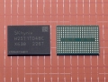
▲SK하이닉스가 지난 3일 공개한 238단 낸드플래시 (사진-SK하이닉스)
SK·마이크론, 200단 적층 경쟁 중 삼성은 침묵
삼성이 바라보는 1000단 미래 낸드, 기술혁신必
[편집자주] 반도체 업계 낸드플래시 적층이 200단을 넘어섰다. 싱글 스택으로 128단을 쌓은 삼성전자 외에는 200단을 넘기 힘들 거라던 지난 말들이 무색하게 적층 경쟁에서 선두에 선 것은 다름아닌 232단을 쌓아 올린 미국의 마이크론이었다. SK하이닉스가 이에 질세라 238단 낸드 플래시 상용화를 예고하며 200단대 선두 싸움에 뛰어들었다. 삼성은 올 초 172단 7세대 V낸드를 UFS 4.0에 탑재하며 관망하는 모양새지만 200단대 기술 확보는 이미 완료됐다며 자신감을 내비쳤다. 200단 낸드 시대, 반도체 제조사들의 격돌을 살펴봤다.
■불붙은 적층 경쟁, 200단 돌파
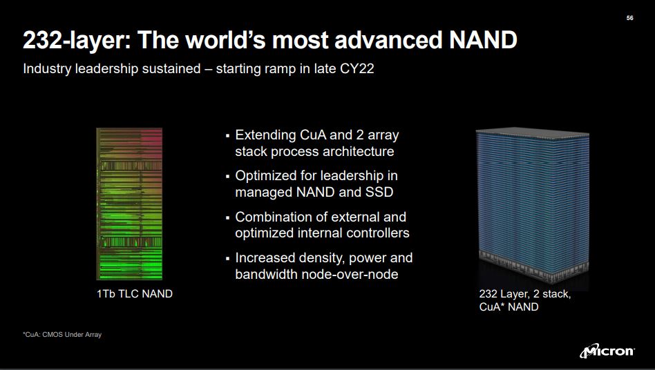
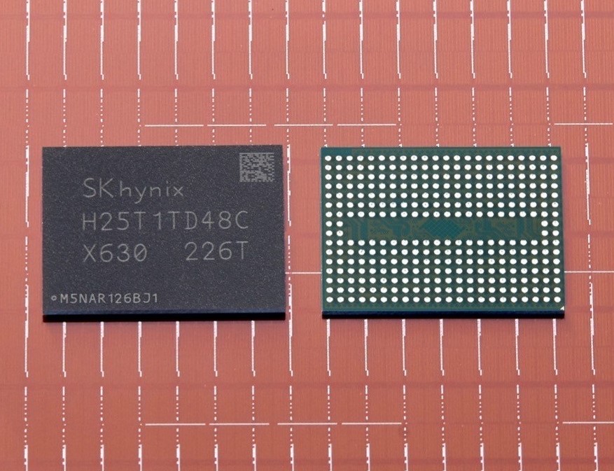
▲마이크론 232단 낸드플래시 발표 (이미지-마이크론테크놀로지)
삼성전자가 2013년 24단 1세대 3D 낸드를 발표한 이후 수평 방향으로 셀을 배열하는 것보다 수직 방향으로 셀을 쌓는 3D 낸드 플래시는 업계 표준 방식이 됐다. 이는 집적도를 올리고 면적은 줄일 수 있어 현재는 모든 제조사가 셀 적층에 열을 올리고 있다.
마이크론테크놀로지(이하 마이크론)가 232단 낸드플래시를 7월 말 공개하며 200단 시대의 포문을 열었다. 세계 최초로 200단대 낸드플래시 양산에 들어가며 기술 선두 타이틀을 획득한 것이다. 이전 세대인 176단 대비 45% 높은 밀도, 28% 더 작은 가로세로 11.5×13.5mm의 개선된 면적의 패키징을 실현시킨 마이크론이었다.
이에 SK하이닉스는 재빨리 238단 낸드플래시 개발 소식을 최근 전해왔다. 마이크론에 비해 6단 높지만 아직 양산 단계에 이른 것은 아니다. 마이크론은 자사 블로그를 통해 “혁신적인 반도체 설계의 프로토 타입을 제작하는 것은 실제로 어렵지만, 3D 낸드를 대량 생산에 적용하는 것은 훨씬 더 큰 도전”이라며 개발보다 양산체제의 실현이 더 큰 고비임을 부각시켰다.
SK하이닉스는 현재 샘플 제품을 고객사에 선보인 것으로 전해지며 내년 상반기에 양산에 들어갈 계획이다. SK하이닉스 관계자는 “단수를 높여 가로세로 면적을 최소화했으며 이에 세계에서 가장 작은 사이즈의 낸드플래시를 구현했다”고 피력했다. 이는 셀을 더 적층해 단위 용량을 높인 만큼 면적을 축소할 수 있었으며, 이로 인해 이전 세대인 176단 대비 생산성은 34% 증가시킬 수 있었다.
중국의 메모리 기업 YMTC도 최근 4세대 3D 232단 낸드 개발에 성공했다고 밝혔다. 칭화유니그룹을 모회사로 둔 YMTC는 중국 정부가 소유한 국영 반도체 회사로 중국의 반도체 굴기 아래 전폭 지원을 받으며 적층 경쟁에 나서고 있는 것이다.
삼성전자는 이러한 200단 경쟁에서 상대적으로 제품 출시가 늦어지는 상황이다. 지난 5월 삼성전자는 7세대 176단 V낸드를 적용한 UFS 4.0 규격 메모리를 개발을 알렸다. 삼성의 7세대 176단 V낸드는 100단 초반대 6세대 V낸드와 높이가 비슷해 최소 셀 크기를 구현했다.
이처럼 뛰어난 기술력과 싱글스택 중 가장 높은 128단 싱글스택 낸드플래시를 보유한 삼성이 가장 먼저 200단대 낸드플래시 양산에 들어갈 것이라는 예상과는 달리 여전히 200단대 제품 양산 소식은 들리지 않고 있다. 이미 더블스택이 적용된 230단대 제품을 공개한 SK하이닉스와 마이크론도 싱글스택으로 128단을 구현할 수 있는 기술력은 확보한 상태인 것이다.
삼성은 지난해 송재혁 메모리사업부 플래시 개발실장의 기고문을 통해 “삼성전자의 V낸드는 1000단 이상을 바라본다”고 선언했다. 이미 기술적으론 200단이 넘는 8세대 V낸드 동작 칩을 확보한 상황으로 시장 상황과 고객 요구에 따라 적기에 제품을 선보일 수 있도록 준비 중에 있다고 설명했다. 이러한 기고로부터 1년이 지난 시점에서 경쟁기업의 200단 낸드 양산 계획이 잇따르고 있지만 삼성전자의 200단대 낸드는 여전히 침묵 중이다.
■1000단 낸드 미래, 적층 한계의 극복 必
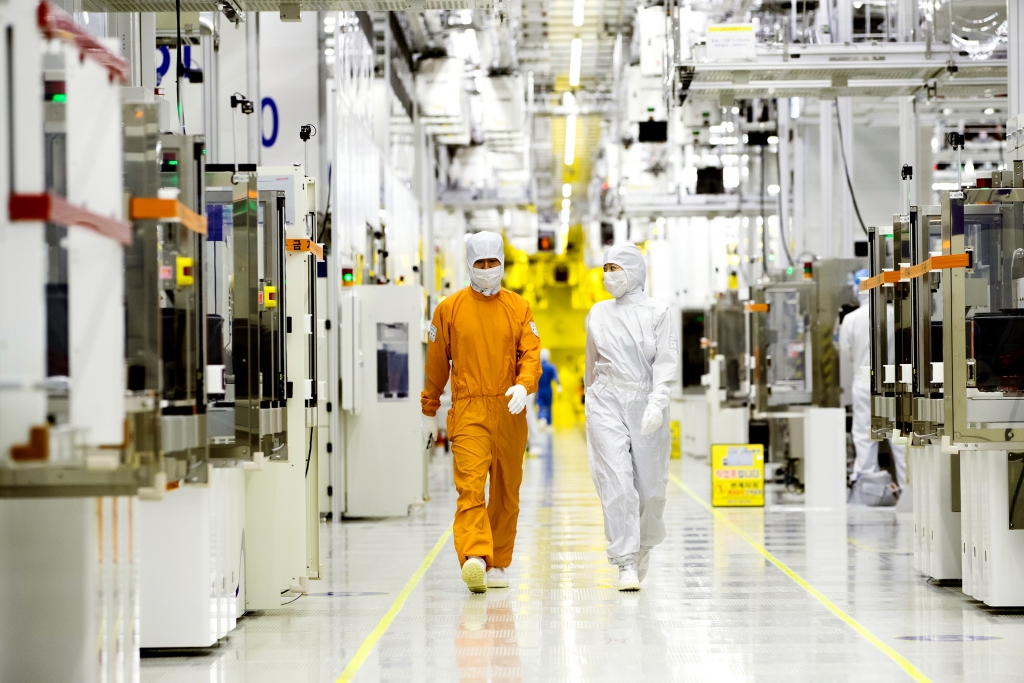
▲삼성전자 클린룸 반도체 생산현장 (사진-삼성전자)
송재혁 삼성전자 메모리사업부 플래시 개발실장은 지난해 기고문에서 삼성전자 V낸드의 미래를 1000단 이상까지 바라본다고 밝혔다. 그는 “3차원 스케일링 기술을 통해 언젠가 마주하게 될 높이의 한계를 가장 먼저 극복할 것”이라며 미래 1000단 V낸드 시대에서 이뤄낼 삼성전자의 기술 혁신을 자신했다.
반도체 업계는 셀 적층 단수가 높아짐에 따라 기술적 문제를 해결해야 하는 상황에 직면하게 된다. 이와 함께 기술적으로 구현이 가능하더라도 수율, 생산성 문제 등 양산화를 위한 공정의 성숙도가 뒷받침돼야 한다.
3D 낸드 적층에는 여러 얇은 층을 증착해야 하는데 단수가 높아질수록 각 셀 사이의 편차가 발생할 수 있다. 이러한 편차가 제품 성능에 영향을 미치며 또한 층이 너무 많으면 무너질 가능성도 커진다. 그렇기에 충격에 견딜 수 있는 내구성을 요하며 설계 난이도도 올라가게 된다.
SK하이닉스는 뉴스룸을 통해 적층에 있어서 무엇보다 어려운 것은 플러그(Plug) 공정이라고 밝힌 바 있다. 플러그 공정은 Oxide/Nitride 스택(ON 스택)을 겹겹이 쌓은 것을 뚫는 공정이다. 적층 단수가 높아질수록 동일한 플러그 사이즈로 더 깊은 구멍을 뚫어야 한다.
이때 내부에 소자 동작을 위한 반도체 박막을 형성해야 하는데 깊이가 깊을수록 균일한 회로선폭을 형성하기가 어려운 것이다. 아무리 정교한 애칭(Etching) 기술이더라도 상부와 하부 회로선폭 간에는 두께 및 형태 차이가 발생하게 되고 이는 하부 소자에 지속적인 스트레스가 인가될 수 있다고 설명했다.
SK하이닉스 관계자는 본지와의 전화통화에서 “과거 더블스택이 적용된 72단 제품이 나왔을 때도 36단의 싱글스택 수준에서 향후 100단 후반대가 나올 수 있느냐는 의문이 많았다”며 “공정 기술혁신에 따라 셀을 애칭하는 장비나 설계 기술의 발전을 통해 몇백단 이상을 바라보게 됐다”고 말했다.