■ MOSFET을 병렬로 사용할 때 고려해야 하는 점이 있나
고전력 모터 드라이브, 서버, 텔레콤 등과 같이 시스템에서 필요로 하는 높은 부하 전류에 대응하기 위해서 MOSFET을 병렬로 연결하여 사용한다.
이론적으로 또는 시뮬레이션 상에서 전체 부하 전류가 MOSFET 병렬 개수만큼 나누어져서 각 MOSFET에 동일한 전류가 흐른다고 가정하여 계산 또는 시뮬레이션을 하고 있지만, 실제 애플리케이션에서는 생산되는 MOSFET이 가지고 있는 특성값의 편차, 공간적 제약에 따른 PCB 배선 패턴의 차이로 인하여 전류의 불균형이 발생될 수 있다.
따라서 제품 설계 시 사용되는 MOSFET의 특성값 편차는 제품마다 보정을 할 수 없지만, 특성값의 Min-Max 값에 대해서 충분히 검토해야 할 필요가 있다.
MOSFET 데이터시트에는 제품과 관련된 여러 가지 특성값이 있는데, 그 중에서 게이트 임계 전압인 VGS(th)값이 MOSFET을 병렬로 사용할 때 고려해야 하는 중요한 파라미터라고 할 수 있다.
■ MOSFET 파라미터 차이가 병렬 MOSFET들 간에 전류 불평형에 어떤 영향을 끼치나
MOSFET은 켜졌을 때 전류가 흐르고 꺼졌을 때 전류가 흐르지 않는 특성을 가지고 있다.
MOSFET 파라미터의 차이로 인하여 병렬로 연결된 MOSFET들 간에 흐르는 전류의 불평형은 앞에서 말한 VGS(th)값의 차이가 주요 원인이 될 수 있다.
VGS(th)가 낮다는 것은 MOSFET이 먼저 켜지거나 나중에 꺼진다는 것을 의미하고, 반대로 VGS(th)가 높다는 것은 MOSFET이 나중에 켜지고 먼저 꺼진다고 생각하면 쉽게 이해하실 수 있다.
따라서 스위칭 동작 시 먼저 켜지고 나중에 꺼지는 VGS(th)가 낮은 MOSFET쪽으로 전류의 쏠림이 발생하게 된다.
■ 시스템 전력 소모를 분석하기 위한 요소와 고려해야 하는 점에 대해 설명 부탁드린다
전력 소모를 분석하기 위한 요소로서는 MOSFET이 켜진 상태에서 흐르는 전류를 알아야 하고, MOSFET이 켜지고 꺼지는 해당 시간 동안의 전압 및 전류 변화를 알아야 한다.
이 부분을 MOSFET 데이터시트의 특성값을 이용하여 계산을 하거나, 또는 당사 홈페이지에서 제공하는 MOSFET 시뮬레이션용 모델을 이용하여 회로를 구성하고 확인하는 방법이 있다.
특히 시뮬레이션을 이용하여 전력 소모를 구할 때는 PCB 배선의 인덕턴스 및 온도 등을 같이 고려하면 조금 더 정확한 결과를 얻을 수 있다.
실제 애플리케이션 상태에서는 오실로스코프를 이용하여 파형을 캡처하고, 이를 이용하여 분석하는 것도 하나의 방법이 될 수 있다.
■ 전력 소모 불평형과 게이트 임계 전압 {VGS(th)} 차이가 미치는 영향은 무엇인가
MOSFET 파라미터 중 VGS(th)값의 차이로 인하여 병렬로 연결된 MOSFET들 간에 흐르는 전류의 불평형이 발생하면 낮은 VGS(th)값을 가지는 MOSFET으로 전류가 많이 흐르게 되고, 이에 따른 도통 손실 및 스위칭 손실이 증가하여 전체 손실이 커지게 된다.
또한, 손실이 크다는 것은 온도 증가가 크다는 것을 의미한다.
따라서 손실·온도가 높아 스트레스가 많이 가해지는 MOSFET에 대한 신뢰성이 감소하게 될 것이고, 경우에 따라서는 MOSFET의 고장으로 이어질 수 있어 애플리케이션 제품의 고장이 발생할 확률이 높아진다.
■ 트랜스컨덕턴스(gfs)는 전류 공유에 어떠한 영향을 끼치나
MOSFET 파라미터 중 하나인 트랜스컨덕턴스는 게이트-소스 간 전압의 변화량에 따른 드레인 (drain) 전류의 변화량을 의미한다.
따라서 게이트-소스 간 전압의 변화가 크면 드레인 전류의 변화량이 크다고 볼 수 있으며, 이 값이 높을수록 전류 공유에 있어 불균형이 증가하는 경향이 있다고 할 수 있다.
■ 인피니언 최신 세대 전력 MOSFET의 특징에 대해 설명 부탁드린다
인피니언의 중전압 MOSFET은 VGS(th) 범위가 일반적으로 제공되는 범위보다 적게 분포되고 관리되고 있어 MOSFET을 병렬로 사용하는 데 있어 다양한 장점을 제공한다.
특히 최신 세대인 OptiMOS™ 6세대는 기존 5세대 제품에 비해서 향상된 온저항 RDS(on) 및 FOM (Figure of merits – RDS(on) x Qg / Qgd)을 달성했다.
이 부분으로 인해 개발자는 낮은 도통 손실과 스위칭 손실을 통해서 시스템의 효율을 올릴 수 있고, 발열에 대한 부분에서도 조금 더 자유로워질 수 있다.
또한 MOSFET 병렬 수를 줄일 수 있어 시스템 단가를 낮추는 데 기여할 수 있다.
나아가서는 스위칭 주파수를 빠르게 가져갈 수 있어 작은 용량의 인덕터 및 커패시터를 사용해 솔루션 사이즈를 줄일 수 있는 이점을 제공한다.
따라서, OptiMOS™ 6세대 제품은 SMPS 애플리케이션에서 낮은 부하 상태와 높은 부하 상태 간의 균형을 유지하면서, 광범위한 출력 전력 시스템에서 효율성을 최적화하는 완벽한 솔루션이라고 할 수 있다.
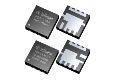
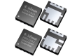
현재 OptiMOS™ 6세대는 40V 및 100V 제품이 출시되었고, 60V, 80V, 120V, 150V, 200V 제품들이 개발 중에 있다.
SuperSO8 5x6mm, PQFN 3.3x3.3mm, sTOLL 7x8mm와 같은 다양한 패키지를 제공하여 시스템 개발에 있어 높은 자유도를 제공한다.