반도체 업계에서는 무어의 법칙 달성을 위해 차세대 첨단 패키징 속에서 그 해답을 찾고 있다. 이에 인텔이 더 큰 확장성을 가질 수 있는 '유리' 소재에서 그 실마리를 찾았다.
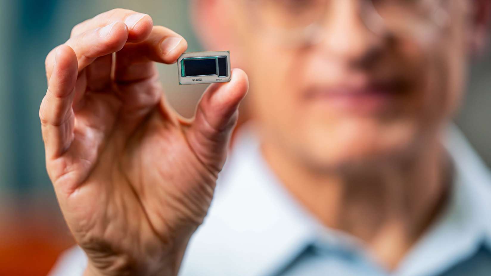
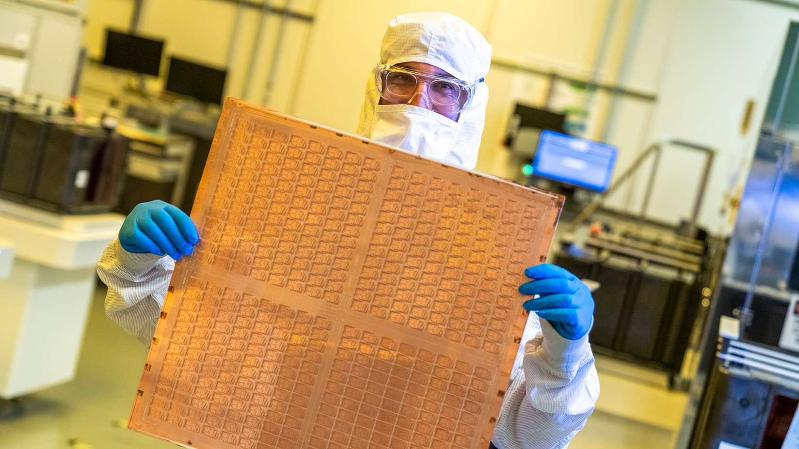
▲인텔이 조립한 유리 기판 테스트 칩을 들고 있는 하미드 아지미(Hamid Azimi) 인텔 부사장 겸 기판 기술 개발 이사(사진:인텔)
2030년 유기 재료 사용 패키징에 한계 전망
유리 기판, 확장성·성능·집적도 대폭 개선 가능
2030년 단일 패키지 내 1조개 트렌지스터 집적
반도체 업계에서는 무어의 법칙 달성을 위해 차세대 첨단 패키징 속에서 그 해답을 찾고 있다. 이에 인텔이 더 큰 확장성을 가질 수 있는 '유리' 소재에서 그 실마리를 찾았다.
인텔이 19일 차세대 첨단 패키징을 위한 업계 최초의 유리 기판 중 하나를 발표했다. 해당 유리 기판은 2030년 내 출시 예정인 것으로 전해졌다.
오늘날의 유기 기판에 비해 유리는 매우 낮은 평탄도, 더 나은 열적(thermal) 및 기계적 안정성과 같은 뛰어난 특성을 제공해 기판의 상호 연결 밀도를 훨씬 더 높일 수 있다. 이러한 이점을 바탕으로 칩 설계자는 AI와 같은 데이터 집약적인 워크로드용 고밀도 및 고성능 칩 패키지를 만들 수 있는 것이다.
인텔은 2030년 안에 완전한 유리 기판 솔루션을 시장에 선보일 계획이다. 2030년까지 반도체 산업은 유기 재료를 사용해 실리콘 패키지의 트랜지스터를 확장하는 데 한계에 도달할 가능성이 높다. 유기 재료는 더 낮은 전력효율성 및 수축과 뒤틀림과 같은 한계를 지닌다. 반도체 산업의 발전과 진화에 있어 확장성은 결정적이며, 유리 기판은 차세대 반도체를 구현하기 위해 실행 가능한 필수적인 단계인 것으로 인텔은 설명했다.
▲유리 기판 테스트 패널(사진:인텔)
더욱 강력한 성능에 대한 요구가 높아지는 가운데 반도체 산업이 여러 개의 ‘칩렛’을 하나의 패키지 내에 탑재하는 이기종 시대로 진입함에 따라, △패키지 기판의 신호 속도 △전원 공급 △설계 규칙 △안정성 개선이 필수적인 요소가 됐다.
유리 기판은 더 많은 트랜지스터를 패키지 내에서 연결할 수 있는 우수한 기계적·물리적·광학적 특성을 보유한다. 더불어, 현재 업계에서 사용 중인 유기 기판 대비 더 나은 확장성을 제공하고, 더 큰 시스템-인-패키지로 불리는 칩렛 복합체 조립을 가능하게 한다. 칩 설계자들은 단일 패키지 내에서 더 작은 공간에 더 많은 타일(혹은 칩렛)을 탑재할 수 있을 뿐 아니라 더 뛰어난 유연성과 낮은 전체 비용 및 전력 사용으로 향상된 성능 및 집적도를 달성할 수 있다.
유리 기판 도입은 △데이터 센터 △인공지능 △그래픽 등 대형 폼팩터를 필요로 하는 워크로드 및 애플리케이션을 다루고, 빠른 속도를 요구하는 산업에서 먼저 채택할 것으로 예상된다.
유리 기판의 특징은 고온 내구성을 가지고 있으며, 패턴 왜곡 발생률이 50% 낮다. 또한, 평탄도가 매우 낮아 리소그래피의 초점 심도를 개선하며, 매우 촘촘한 레이어 간 인터커넥트 오버레이에 필요한 구조적 안정성을 갖추고 있다. 이러한 독특한 특성으로 인해 유리 기판에서 인터커넥트 밀도를 10배 높일 수 있다. 나아가, 유리가 가진 개선된 기계적 특성은 매우 높은 조립 수율로 초대형 폼팩터 패키지 구현을 가능하게 한다.
유리 기판의 고온 내구성은 칩 설계자에게 전원 공급 및 신호 라우팅에 보다 유연한 설계 규칙을 적용하게 한다. 이는 광학 인터커넥트를 원활하게 통합하고, 유리 내에 인덕터와 캐패시터를 더 높은 온도에서 처리할 수 있는 역량을 제공한다. 따라서, 더 나은 전원 공급 솔루션을 구현하면서도 더 낮은 전력에서 필요한 속도의 신호를 제공하게 된다. 이러한 이점으로 2030년까지 단일 패키지 내에서 1조 개의 트랜지스터를 집적하려는 목표에 한 발 더 다가설 수 있다.
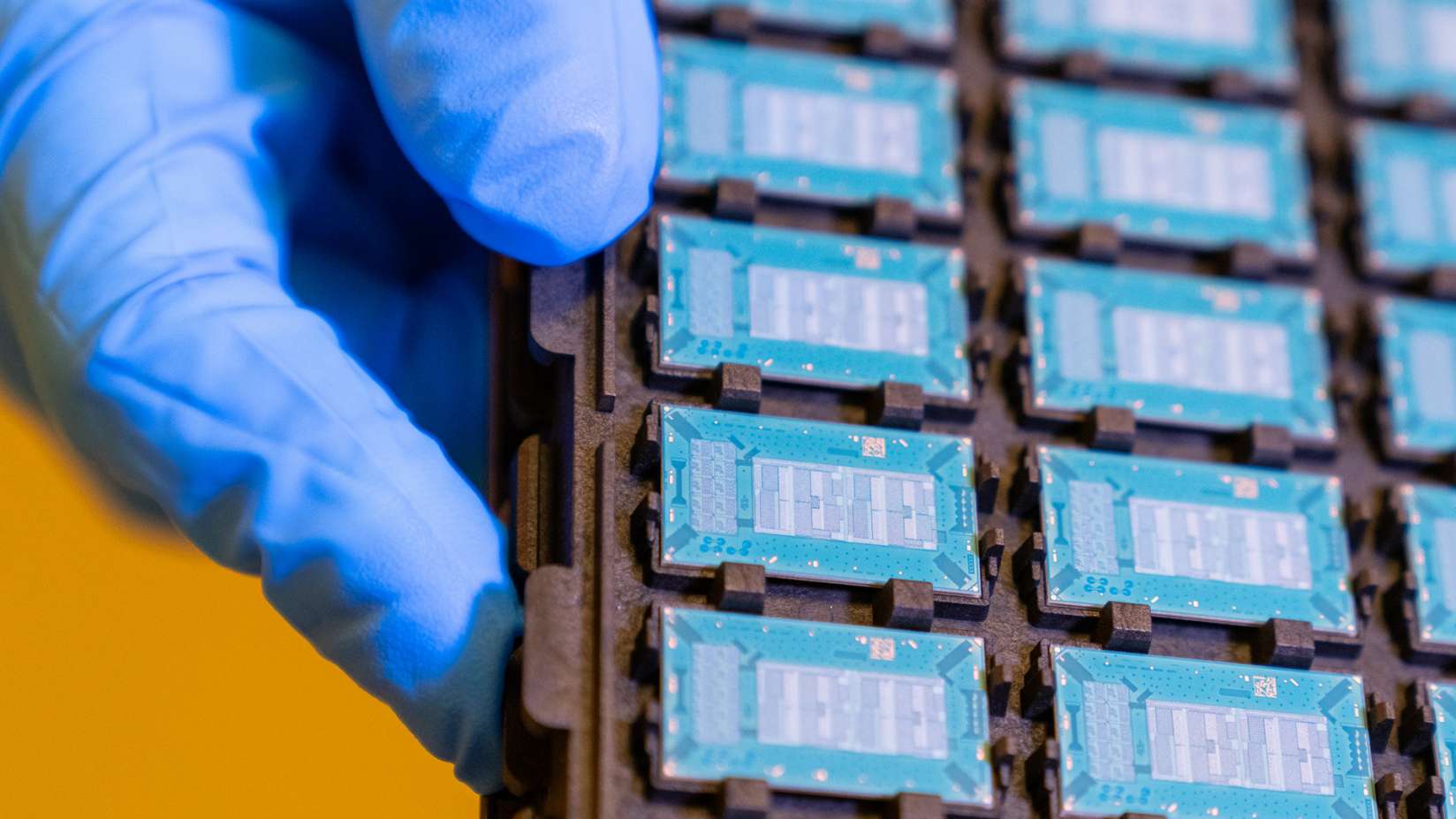
▲유리 기판 테스트 패널(사진:인텔)
인텔은 지난 10년 이상 동안 유기 기판 대체재로서의 유리 기판의 신뢰성을 연구하고 검증해왔다. 인텔은 1990년대 세라믹 패키지에서 유기 패키지로의 전환을 주도했으며, 할로겐(halogen)과 무연 패키지를 최초로 선보였다. 또한, 고급 임베디드 다이 패키징 기술을 개발해 업계 최초의 활성 3D 집적 기술을 구현했다. 인텔은 이러한 혁신적인 기술을 중심으로 장비, 화학물질, 원자재 공급 업체부터 기판 제조업체를 아우르는 전체 생태계를 활성화시킬 수 있었다.
인텔 조립 및 테스트 기술 개발 부문 총괄 바박 사비(Babak Sabi)부사장은 “10년간의 연구 끝에 인텔은 첨단 패키징에 활용할 업계 선도적인 유리 기판을 확보했다”며 “앞으로 수십 년간 주요 업체 및 파운드리 고객이 수혜를 누릴 수 있는 최첨단 기술을 선보일 것으로 기대한다”고 말했다.
한편, 인텔은 최근 파워비아(PowerVia) 및 리본펫(RibbonFET) 등 획기적인 기술에 이어 업계 선도적인 유리 기판을 첨단 패키징에 사용함으로써 인텔 18A 공정 노드를 넘어서는 차세대 컴퓨팅을 향한 노력을 입증했다. 인텔은 2030년까지 단일 패키지 내에 1조개의 트랜지스터를 집적하기 위해 노력 중이며, 유리 기판을 비롯 첨단 패키징 분야에서 지속적인 혁신을 통해 목표를 달성할 예정이다.