기사입력 2024.02.28 08:01
.jpg)
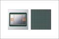
삼성전자가 로직과 HBM 4개를 단일 패키지로 통합하는 2.5D 패키지 기술, ‘I-Cube4’를 개발했다. 해당 기술은 고대역폭 데이터 전송과 고성능 시스템 반도체를 요구하는 HPC, AI/클라우드 서비스, 데이터센터 등을 중심으로 활용될 것으로 기대된다.
2021-05-06 오전 11:01:24by 이수민 기자
국내외 AI 반도체 및 데이터센터 등 AI 시장 핵심 인프라에 대한 투자가 촉진되고 있다. 삼성전자는 2021년 메모리 반도체와 AI 프로세서를 하나로 결합한 ‘HBM-PIM’을 지속 발전시키고 있다. SK하이닉스는 AI 추론·학습 성능에 최적화된 차세대 적층형 메모리 ‘HBM3’ 개발에 성공했다. 데이터센터는 빅데이터를 수집·저장·분석할 수 있는 클라우드 컴퓨팅 서비스를 제공하며, AI 모델을 훈련하는 데 적합하다. 국내에서 AI 반도체 개발과 함께 안정적인 인프라 확보를 위한 데이터센터 투자가 가속화되고 있다.
2023-03-06 오후 4:39:03by 김예지 기자

인공지능 기술과 소프트웨어로 기능하는 자동차 등 디바이스에서 요구하는 데이터양이 막대해지고 있다. 늘어나는 데이터 양에 대응하고 이러한 데이터를 활용할 수 있는 기술을 갖추는 데 시장 니즈가 높아지고 있는 가운데 단순히 데이터 처리 속도를 만족하면서 처리할 수 있는 데이터 양까지 충족하기 위해선 프로세서를 지원하는 메모리 속도가 필수적으로 뒷받침돼야 한다.
2023-06-12 오후 12:25:04by 권신혁 기자
.jpg)
2분기 메모리 반도체 실적은 모바일, PC 등 소비자향 제품 및 일반 서버의 저조한 수요 회복으로 연이은 적자를 기록했다. 다만 AI 서버 시장의 활황으로 HBM3와 DDR5 등 고부가가치 라인업에서 수주 확대가 이뤄져 점진적 회복이 전망되고 있다.
2023-07-26 오전 11:04:23by 권신혁 기자
시장조사업체 트렌드포스는 1일 AI 가속기 칩 수요가 증가하고, 업체들이 자체 칩을 개발하는 추세에 따라 2024년 새로운 HBM3·HBM3e이 시장의 주류가 될 것이라 주장했다. 엔비디아의 거세진 입김을 피하기 위해 최근 업계는 자체 AI 칩 개발에 몰두하고 있다. AI 가속기 칩에 대한 수요가 진화함에 따라 HBM3 및 HBM3e의 성장이 예측된다.
2023-08-03 오후 1:30:08by 김예지 기자
.jpg)
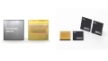
SK하이닉스는 21일 AI용 초고성능 D램 신제품인 ‘HBM3E’를 개발하고, 성능 검증 절차를 진행하기 위해 고객사에 샘플을 공급하기 시작했다.
2023-08-21 오후 12:57:23by 김예지 기자

AI향 반도체에 필수적인 차세대 메모리 HBM3로 주가를 올리고 있는 SK하이닉스가 창립 40주년을 맞이했다. 이에 창립 기념 특별대담에서 곽노정 대표이사가 미래 반도체 기술 전망과 SK하이닉스의 비전을 밝혔다.
2023-10-10 오후 3:40:47by 권신혁 기자
처리 속도를 혁신적으로 끌어올리기 위해 등장한 ‘HBM(High Bandwidth Memory)’은 여러 개의 D램을 TSV(실리콘 관통 전극) 기법으로 수직 연결한 고대역폭 메모리다. HBM 시장은 삼성전자와 SK하이닉스가 양대 산맥을 차지하고 있으며, 마이크론이 이를 뒤쫓고 있다. 트렌드포스에 따르면 지난해 글로벌 HBM 시장 점유율은 SK하이닉스가 50%, 삼성전자(40%), 마이크론(10%)으로 나타났다. 2026년 엔비디아 및 아마존, 구글, MS 등과 같은 클라우드 서비스 제공사(Cloud Service Provider, CSP)의 수요에 맞춰 출시될 HBM4는 지금의 반도체와는 다른 방식이 도입된다.
2023-11-30 오후 4:53:35by 김예지 기자
SK하이닉스가 최근 지난 4분기 실적에서 3,460억원의 영업이익 흑자전환을 이뤘다고 발표했다. 이에 1년 여만에 실적 회복 흐름이 2024년에도 강하게 이어질 것으로 점쳐진다.
2024-01-29 오후 4:49:39by 권신혁 기자

[열린보도원칙] 당 매체는 독자와 취재원 등 뉴스이용자의 권리 보장을 위해 반론이나 정정보도, 추후보도를 요청할 수 있는 창구를 열어두고 있음을 알려드립니다.
고충처리인 장은성 070-4699-5321 , news@e4ds.com


