삼성전자, ‘9세대 V낸드’ 업계 최고 단수 쌓았다
기사입력 2024.04.23 16:13
더블 스택 구조, 채널 홀 에칭으로 공정 혁신
하반기 QLC 9세대 V낸드 양산, AI 수요 대응
하반기 QLC 9세대 V낸드 양산, AI 수요 대응
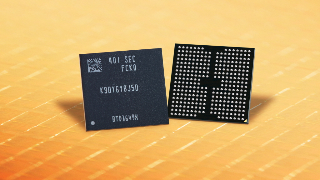
삼성전자가 더블 스택 구조로 구현 가능한 최고 단수를 쌓은 9세대 V낸드 양산에 성공하며 메모리 반도체 기술 리더십을 증명했다.
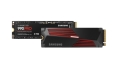
삼성전자는 업계 최초로 ‘1Tb(테라비트) TLC(Triple Level Cell) 9세대 V낸드’ 양산을 시작했다고 23일 밝혔다.
TLC(Triple Level Cell)는 하나의 셀에 3bit 데이터를 기록할 수 있는 구조다.
삼성전자는 △업계 최소 크기 셀(Cell) △최소 몰드(Mold) 두께를 구현해 ‘1Tb TLC 9세대 V낸드’의 비트 밀도(Bit Density)를 이전 세대 대비 약 1.5배 증가시켰다.
더미 채널 홀(Dummy Channel Hole) 제거 기술로 셀의 평면적을 줄였으며, 셀의 크기를 줄이면서 생기는 간섭 현상을 제어하기 위해 셀 간섭 회피 기술, 셀 수명 연장 기술을 적용해 제품 품질과 신뢰성을 높였다.
삼성전자의 ‘9세대 V낸드’는 더블 스택(Double Stack) 구조로 구현할 수 있는 최고 단수 제품으로, ‘채널 홀 에칭(Channel Hole Etching)’ 기술을 통해 한번에 업계 최대 단수를 뚫는 공정 혁신을 이뤄 생산성 또한 향상됐다.
삼성전자는 정확한 층수는 밝히지 않았지만 시장은 290단 이상이 될 것으로 추측하고 있다.
‘채널 홀 에칭’이란 몰드층을 순차적으로 적층한 다음 한번에 전자가 이동하는 홀(채널 홀)을 만드는 기술이다. 특히, 적층 단수가 높아져 한번에 많이 뚫을수록 생산효율 또한 증가하기 때문에 정교화·고도화가 요구된다.
‘9세대 V낸드’는 차세대 낸드플래시 인터페이스인 ‘Toggle 5.1’이 적용돼 8세대 V낸드 대비 33% 향상된 최대 3.2Gbps의 데이터 입출력 속도를 구현했다. 삼성전자는 이를 기반으로 PCIe 5.0 인터페이스를 지원하고 고성능 SSD 시장을 확대해 낸드플래시 기술 리더십을 공고히 할 계획이다.
또한 ‘9세대 V낸드’는 저전력 설계 기술을 탑재하여 이전 세대 제품 대비 소비 전력이 약 10% 개선됐다. 환경 경영을 강화하면서 에너지 비용 절감에 집중하는 고객들에게 최적의 솔루션이 될 것으로 기대된다.
삼성전자 메모리사업부 Flash개발실장 허성회 부사장은 “낸드플래시 제품의 세대가 진화할수록 고용량·고성능 제품에 대한 고객의 니즈가 높아지고 있어 극한의 기술 혁신을 통해 생산성과 제품 경쟁력을 높였다”며 “9세대 V낸드를 통해 AI 시대에 대응하는 초고속, 초고용량 SSD 시장을 선도해 나갈 것”이라고 밝혔다.
삼성전자는 ‘TLC 9세대 V낸드’에 이어 올 하반기 ‘QLC(Quad Level Cell) 9세대 V낸드’도 양산할 예정으로 AI시대에 요구되는 고용량·고성능 낸드플래시 개발에 박차를 가할 계획이다.

관련뉴스
-
삼성전자, 메모리 로드맵 공개…10나노 D램·1,000단 낸드 개발
“삼성전자가 약 40년간 만들어낸 메모리의 총 저장용량이 1조 기가바이트(GB)를 넘어서고, 이중 절반이 최근 3년간 만들어졌을 만큼 우리는 급변하는 디지털 전환을 체감하고 있다”
2022-10-07 오전 10:10:35by 권신혁 기자
-
.jpg)
삼성전자, ‘1Tb TLC 8세대 V낸드’ 양산
삼성전자가 웨이퍼당 비트 집적도를 대폭 향상시킨 세계 최고 용량의 8세대 V낸드 양산에 들어가며, 차세대 서버 시장의 고용량화 주도와 함께 고신뢰성을 요구하는 전장 시장까지 V낸드 사업 영역을 확대한다.
2022-11-07 오후 2:13:28by 배종인 기자
-

키옥시아·WD, 218단 낸드 출시
키옥시아(Kioxia)와 웨스턴디지털(Western Digital, 이하 WD)이 합작한 최신 3D 플래시 메모리 기술의 세부 정보가 공개됐다.
2023-03-31 오후 2:44:17by 권신혁 기자
-

2분기 D램·낸드 ASP 하락폭 확대
메모리 시장이 2분기를 정점으로 감산 및 신규 수요를 통한 재고 축소가 이뤄질 것으로 예상한 가운데 D램과 낸드플래시 평균판매가격(ASP)이 당초 예상치를 뛰어넘는 하락폭을 보이고 있다는 소식이 전해졌다.
2023-05-10 오전 10:16:53by 권신혁 기자
-
SK하이닉스, 세계 최고층 238단 4D 낸드 양산 돌입
SK하이닉스가 세계 최고층 238단 4D 낸드 양산을 통해 하반기 경영실적 반등을 꾀한다.
2023-06-08 오전 9:58:20by 배종인 기자
-
SK하이닉스, 세계 최고층 321단 낸드 샘플 공개
SK하이닉스가 ‘321단 4D 낸드’ 샘플을 공개하며 업계 최초로 300단 이상 낸드 개발을 진행중이라고 공식화했다.
2023-08-09 오전 8:01:54by 권신혁 기자
-
삼성전자, 고성능 SSD ‘990 PRO’ 4TB 출시
삼성전자가 최첨단 8세대 V낸드가 적용되고, PCle 4.0 기반 소비자용 SSD 중 가장 빠른 임의 읽기 속도 제공하는 고성능 SSD를 출시하며 고성능 게임, 3D/4K 그래픽 작업을 전문으로 하는 소비자 공략에 나선다.
2023-09-12 오전 8:56:13by 배종인 기자


많이 본 뉴스
[열린보도원칙] 당 매체는 독자와 취재원 등 뉴스이용자의 권리 보장을 위해 반론이나 정정보도, 추후보도를 요청할 수 있는 창구를 열어두고 있음을 알려드립니다.
고충처리인 장은성 070-4699-5321 , news@e4ds.com