기사입력 2024.08.06 16:25
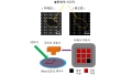
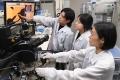
기초과학연구원(IBS, 원장 노도영) 나노입자 연구단 김대형 부연구단장(서울대 화학생물공학부 교수)과 현택환 단장(서울대 화학생물공학부 석좌교수) 연구팀은 최문기 UNIST 교수, 양지웅 DGIST 교수팀과 공동으로 세계 최고 성능의 스트레처블 QLED(퀀텀닷발광다이오드) 개발에 성공했다.
2024-04-16 오전 9:44:12by 배종인 기자
삼성전자가 초대형 디스플레이를 선호하는 시장 트렌드에 따라 마이크로 LED의 라인업이 89형·101형에 이어 114형으로 확대해 소비자 선택 폭을 넓혔다.
2024-05-07 오후 2:19:28by 배종인 기자
산업통상자원부 국가기술표준원(원장 진종욱)이 반도체 소자(IEC TC47) 국제표준 회의에서 광발광(Photoluminescence) 측정법을 활용한 비접촉식 마이크로 LED 소자 품질 검사 방법을 국제 표준으로 제안했다.
2024-05-22 오후 3:07:56by 배종인 기자
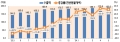
2024년 5월 정보통신산업(ICT) 수출이 반도체, 디스플레이, 휴대폰 등 품목 전반이 수출 호조를 보이며, 190억5,000만달러를 기록 전년동월대비 31.8% 증가했다.
2024-06-18 오전 9:07:10by 배종인 기자
산업통상자원부(장관 안덕근)가 2024년 소부장 핵심전략기술 기술지원 기반구축사업 7개 신규과제를 공모한다. 공모 분야는 △반도체 AI 반도체 공급망 강화를 위한 실증 및 기반구축 △디스플레이 OLED용 고기능 코팅/필름 실증 기반구축 △자동차 미래차용 고출력 전력변화장치의 국산화를 위한 신뢰성 기반구축 △전기전자 차세대 통신부품 공급망 강화를 위한 실증기반 구축 △기계 자율 협업 제조 공정용 제어 모듈 평가 인프라 구축 △금속 수소산업용 고인성·내수소취화 금속소재 실증 기반구축 △기초화학 친환경 바이오 소재 사업화 지원 기반구축 등이다.
2024-07-01 오전 10:45:21by 배종인 기자
한국전기연구원(KERI) 표재연 박사팀이 나노 구조에서 관찰되는 고지향성 발광 패턴을 규명하는데 성공해 초고해상도 디스플레이 분야 기술 혁신이 기대된다.
2024-07-22 오전 11:28:37by 배종인 기자
한국전자통신연구원(ETRI)이 텔레륨(Te) 기반의 칼코지나이드계 p형 반도체 소재를 활용해 상온증착이 가능하면서도 공정이 단순한 p형 Se-Te(셀레늄-텔레늄) 합금 트랜지스터를 개발하며, 향후 차세대 디스플레이 및 초저전력 반도체 소자 성능개선에 널리 활용될 전망이다.
2024-07-24 오후 2:32:27by 배종인 기자

[열린보도원칙] 당 매체는 독자와 취재원 등 뉴스이용자의 권리 보장을 위해 반론이나 정정보도, 추후보도를 요청할 수 있는 창구를 열어두고 있음을 알려드립니다.
고충처리인 장은성 070-4699-5321 , news@e4ds.com