기사입력 2024.11.11 16:00
과학기술정보통신부 산하 한국기계연구원(원장 류석현)은 오는 9월4일 오후 1시10분부터 서울 국회 박물관에서 ‘2024 글로벌 기계기술 포럼’을 온·오프라인으로 동시 개최한다. 과학기술정보통신부와 국가과학기술연구회의 후원으로, 기계연과 국회 더불어민주당 조승래 의원, 국민의힘 최형두 의원, 더불어민주당 황정아 의원이 공동 주최하는 이번 포럼은 디지털 대전환을 주제로 기계기술 관련 국내외 전문가를 초청해 변모하는 미래 기계기술의 발전 방향을 논의한다.
2024-08-26 오전 10:38:16by 배종인 기자
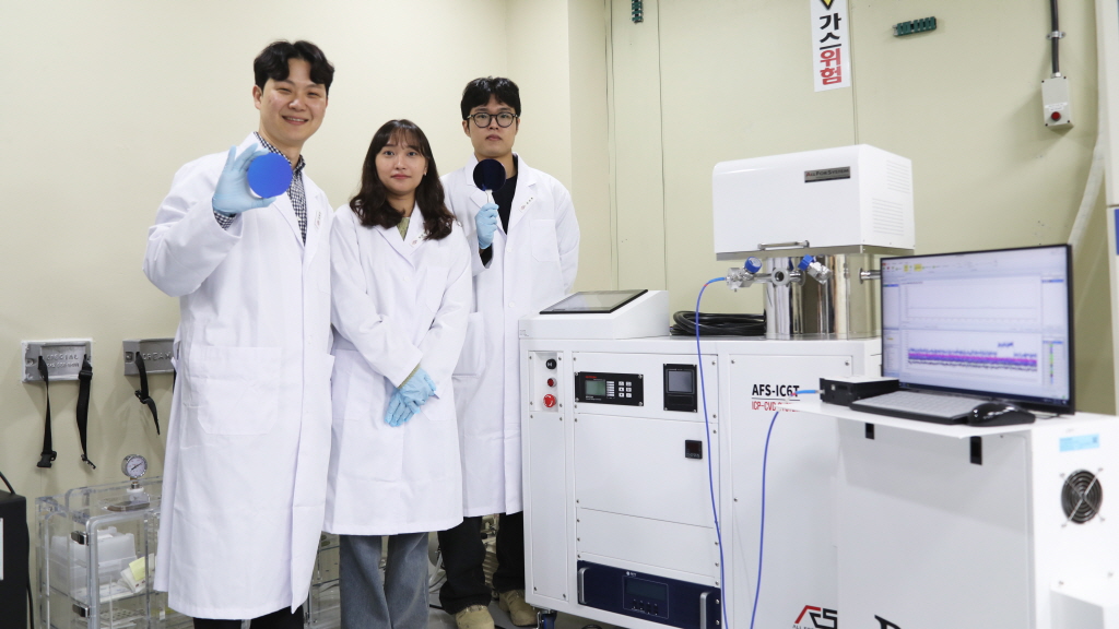
과학기술정보통신부 산하 한국기계연구원(원장 류석현)이 액체 방울의 표면장력 원리를 모사해 강성이 자유자재로 변하는 모핑 휠을 세계 최초로 개발하고, 이를 실제 이동체에 적용하는 데 성공했다. 바퀴의 강성을 실시간으로 변화시켜 계단이나 바위같이 일상생활의 다양한 장애물을 극복할 수 있어 도로 위 장애물 극복이 중요한 휠을 활용하는 모든 이동체에 폭넓게 적용될 수 있을 것으로 보인다.
2024-09-03 오전 1:07:56by 배종인 기자
.jpg)
과학기술정보통신부 산하 한국기계연구원(원장 류석현)은 히트펌프 시장과 정책 동향, 주요 분야별 전략 품목을 담은 기계기술정책 제116호 ‘산업용 히트펌프 동향과 대응 방향’을 발간했다.
2024-09-13 오전 8:55:18by 배종인 기자
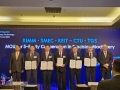
과학기술정보통신부 산하 한국기계연구원(원장 류석현, 이하 기계연)이 체코공대(CTU·Czech Technical University in Prague), 체코 발전소용 부품 가공업체 TGS(TGS·TGS Tools-Machines-Technological Services), 한국산업기술기획평가원(KEIT, 원장 전윤종), 국내 공작기계 제조사 ㈜스맥(SMEC, 대표 최영섭)과 정밀기계 분야 5자 협력 MOU를 체결하고, 동구권 연구협력 기반을 구축했다.
2024-09-23 오전 8:48:16by 배종인 기자
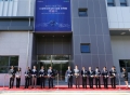
과학기술정보통신부 산하 한국기계연구원(원장 류석현)이 스마트제조장비 실증 실험동을 준공하며, 첨단 기술 상용화 및 제조혁신 성과 창출이 가속화 될 것으로 기대된다.
2024-09-27 오후 2:44:19by 배종인 기자
.jpg)
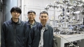
과학기술정보통신부 산하 한국기계연구원(원장 류석현) 부산기계기술연구센터 배승훈 선임연구원 연구팀과 유진에스엠알시오토모티브테크노㈜(유진SMRC A.T., 대표 김흥식), 에스에이치코리아(대표 우상일) 연구팀은 자동차 콕핏 모듈의 에어덕트 제조 기술을 획기적으로 개선했다. 성능평가에서 완성차 규격을 만족해 상용화를 앞두고 있다.
2024-10-03 오전 4:36:11by 배종인 기자
과학기술정보통신부 산하 한국기계연구원(원장 류석현) 에너지저장연구실 임형수 책임연구원 연구팀은 Zero GWP 냉매를 사용한 무급유 방식의 극저온 터보 팽창기를 개발하고 천연가스 액화용 팽창기의 실증 시험을 마쳤다. 이번 영하 183℃ 이하급 극저온 터보 팽창기 개발을 통해 수소, 천연가스 등 대체 에너지를 극저온 상태에서 효율적으로 저장할 수 있어 향후 극저온 냉각시스템 시장에서 해외 의존도를 크게 줄이고, 대체 에너지 저장의 효율을 대폭 향살 시킬 것으로 기대된다.
2024-10-21 오후 3:42:21by 배종인 기자

[열린보도원칙] 당 매체는 독자와 취재원 등 뉴스이용자의 권리 보장을 위해 반론이나 정정보도, 추후보도를 요청할 수 있는 창구를 열어두고 있음을 알려드립니다.
고충처리인 장은성 070-4699-5321 , news@e4ds.com