기사입력 2025.02.18 08:41
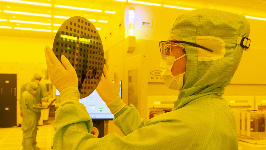
EV 그룹(EVG)은 학계, 연구기관, 산업체를 위한 나노기술 R&D 중심인 나노종합기술원(NNFC)과 원재료 제조 및 공정서비스를 제공하는 NNFC에서 분사한 토탈 솔루션 업체 나노 이니쉐이티브 (NI: Nano Initiative)와 공동으로, 현재 초기 결과들을 비롯해 디스플레이를 위한 개선된 투명 나노 구조화 반사-방지 코팅(nanostructured anti-reflective coating)을 생산하기 위한 공동개발프로그램 (JDP)의 제시 방향을 발표했다. 공동개발프로그램을 진행해온 3사 협력사들은, 대부분의 고분자 코팅(polymeric coatings) 보다 우수한 97 퍼센트 이상의 투과율과 표면경도 3H를 제공하는 뛰어난 구조 복제의 반사방지 코팅(nanostructured anti-reflective coating)을 성공적으로 입증했다. 이와 대조적으로, 현재 박막광학 코팅(thin-film coatings) 기술은 92 퍼센트의 투과율만 제공한다.
2016-07-13 오후 2:33:15by 김수지 기자
자유도와 높은 정밀도로 나노 및 마이크로 광학 부품과 기기를 대량 생산하고자 하는 사용자의 요구를 충족할 수 있는 최첨단 솔루션이 등장했다. EV 그룹(이하 EVG)이 자동화된 SmartNIL® 나노임프린트 및 웨이퍼 레벨 광학 시스템인 EVG®7300을 출시한다.
2022-01-19 오후 12:01:08by 성유창 기자
MEMS, 나노기술, 반도체 시장용 웨이퍼 본딩 및 리소그래피 장비 분야를 선도하는 EV Group이 대만 ITRI에 웨이퍼 본딩 및 리소그래피 장비를 공급하며, 반도체 개발에 서로 협력한다.
2022-09-06 오후 3:16:26by 배종인 기자
.jpg)
MEMS, 나노기술, 반도체 시장용 웨이퍼 본딩 및 리소그래피 장비 전문 기업인 EV Group(이하 EVG)가 새로워진 디자인의 200㎜ 레지스트 처리 장비를 선보이며, 이전 세대의 우수한 성능을 바탕으로 모듈 용량을 늘려 생산성을 높였다.
2022-11-09 오전 9:16:05by 배종인 기자
EVG가 ㈜피엠티(PROTEC MEMS Technology)로부터 자사의 LITHOSCALE® 마스크리스 노광 시스템에 대한 공급 계약을 수주했다.
2024-01-24 오전 9:46:36by 배종인 기자
MEMS, 나노기술, 반도체 시장용 웨이퍼 본딩 및 리소그래피 장비 분야를 선도하는 EV Group이 적외선(IR) 레이저를 적용한 EVG의 레이어 분리 신기술을 통해 첨단 패키징에서 트랜지스터 소형화까지 박막 3D 적층을 실현했다.
2024-02-01 오후 3:18:03by 배종인 기자

[열린보도원칙] 당 매체는 독자와 취재원 등 뉴스이용자의 권리 보장을 위해 반론이나 정정보도, 추후보도를 요청할 수 있는 창구를 열어두고 있음을 알려드립니다.
고충처리인 장은성 070-4699-5321 , news@e4ds.com


