기사입력 2025.03.19 15:10
.jpg)
.jpg)
GMR 다회전 위치 센서용 마그넷 설계 방법에 대해 아나로그디바이스(ADI)의 스티븐 브래드쇼, 크리스티안 나우, 엔다 니콜에게 들어봤다.
2024-01-18 오후 12:02:25by 편집부
공간을 절약하고 효율을 향상하는 4-스위치 벅-부스트 컨트롤러에 대해 아나로그디바이스(ADI)의 슈 장에게 들어봤다.
2024-02-08 오전 11:34:11by 편집부

아나로그디바이스(ADI)가 반도체 파운드리 기업인 TSMC와 장기적인 웨이퍼 공급에 관한 특별 계약을 체결했다고 23일 밝혔다.
2024-02-23 오전 9:44:14by 권신혁 기자

BMW 그룹이 아나로그디바이스(ADI)의 10BASE-T1S 이더넷-대-에지 버스 기술인 E²B™(Ethernet to the Edge bus)를 채택했다.
2024-03-07 오후 4:29:45by 배종인 기자

글로벌 반도체 선도기업인 아나로그디바이스(ADI)와 바이오 플랫폼 혁신 기업인 플래그십 파이어니어링(Flagship Pioneering)이 응용 생물학 및 공학 분야에 대한 양사의 상보적인 전문성을 활용해 여러 디지털 생물학 플랫폼 회사 설립 및 강화에 본격 나선다.
2024-07-29 오후 3:03:52by 배종인 기자
온디바이스 AI 개발을 가속화하기 위해서는 HW-SW 간극을 매꿔주는 임베디드 솔루션이 핵심이다. 이에 MCU 제조사들은 엣지에서의 인텔리전스를 강화하는 기업들의 개발 트렌드에 부합하는 솔루션들을 속속 선보이고 있는 추세이다.
2024-10-08 오전 11:48:14by 권신혁 기자
아나로그디바이스(ADI, Analog Devices)가 한국전자전(KES 2024)에 참가해 산업(Industrial), 오토모티브(Automotive), 소비자(Sonsumer) 부분에서 10개 아이템을 선보이며, 산업용 전자 부품 공급 능력을 과시했다.
2024-10-24 오후 3:51:37by 배종인 기자
.jpg)
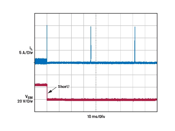
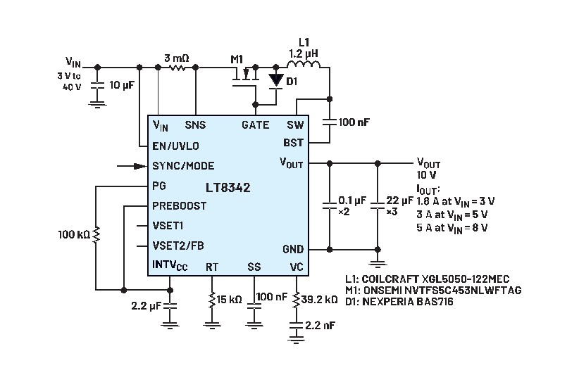
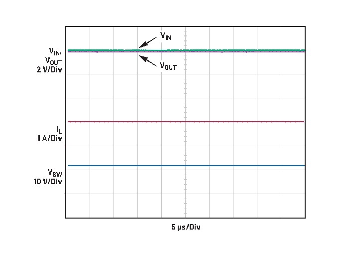
전원관리 시스템 개발을 위한 툴체인에 대해 아나로그디바이스(ADI)의 프레데릭 도스탈에게 들어봤다.
2024-12-06 오후 1:59:23by 배종인 기자
.jpg)
10BASE-T1L 빌딩 컨트롤러를 활용하여 지속 가능한 빌딩 관리 시스템을 구축하는 방법에 대해 아나로그디바이스(Analog Devices, Inc., ADI)의 살렘 가비(Salem Gharbi) 시스템 애플리케이션 엔지니어에게 들어봤다.
2025-02-06 오후 12:13:16by 편집부
.JPG)
ADI Trinamic 모터 제어 솔루션은 StealthChop™, CoolStep™, StallGuard™ 등의 혁신적 기술을 통해 산업 자동화, 의료 기기, 스마트 디바이스 분야에서 정밀도와 에너지 효율성을 동시에 제공하며 AI와의 통합을 통해 지속가능한 모션 컨트롤의 미래를 열어가고 있습니다.
2025-02-18 오후 2:15:30by 명세환 기자
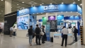
아나로그디바이스(Analog Devices, ADI)가 산업 분야에서의 독보적인 기술력과 혁신적인 AI 솔루션을 바탕으로 산업자동화와 자동차 시장에서 점유율을 높여가고 있는 것으로 나타났다. 이러한 성과를 바탕으로 ADI는 3월12일부터 14일까지 서울 삼성동 코엑스에서 개최되는 ‘오토메이션 월드 2025(AW 2025)’에 참가해 주요 제품을 선보였다.
2025-03-14 오전 10:51:14by 배종인 기자
.jpg)
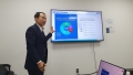
글로벌 반도체 기업 아나로그 디바이스(Analog Devices Inc., 이하 ADI)의 국내 유통 및 기 술지원을 담당하는 마크니카 코리아의 황정필 기술지원 매니저는 지난 14일 서울 삼성동 코 엑스에서 개최된 ‘2025 e4ds 모터제어 기술 컨퍼런스’에서 ADI의 트라이나믹(Trinamic) 솔루 션을 소개하며, ADI가 첨단 산업 자동화 시스템과 스마트팩토리 구현에 필수적인 ADI의 모터 구동 및 제어 기술을 혁신적으로 발전시키고 있다고 밝혔다.
2025-03-19 오후 12:26:35by 배종인 기자

[열린보도원칙] 당 매체는 독자와 취재원 등 뉴스이용자의 권리 보장을 위해 반론이나 정정보도, 추후보도를 요청할 수 있는 창구를 열어두고 있음을 알려드립니다.
고충처리인 장은성 070-4699-5321 , news@e4ds.com