기사입력 2019.10.16 07:02
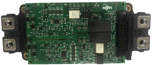
한국전자통신연구원은 산화갈륨을 이용해 2300V 고전압에도 견디는 전력 반도체 트랜지스터를 세계 최초로 개발했다. 기존 전력반도체소자가 실리콘, 질화갈륨, 탄화규소 위에 소자설계 후 패턴작업과 식각, 증착공정을 거쳐 트랜지스터를 만들었다면, 이 기술은 기존 반도체 대신 산화갈륨을 이용한다는 점이 차별점이다. 산화갈륨은 기존 반도체 소재들보다 에너지 밴드 갭이 넓어 고온·전압에서도 반도체 성질을 유지, 칩 소형화와 고효율화가 가능하다. 이 기술은 고전압이 요구되는 전자제품, 전기자동차, 풍력발전, 기관차 등에서 전력을 바꿔주는 모듈에 사용됨으로써 고전압·전력에서도 잘 견디는 힘센 반도체로서의 역할이 가능할 것으로 보인다.
2019-05-19 오전 10:02:05by 이수민 기자
.png)
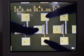
KETI가 스마트팩토리 무인이송로봇의 자율주행을 위한 SLAM용 스캐닝 라이다 센서 국산화에 성공했다. 과거 AGV는 바닥에 부착된 광학인식용 금속선이나 마그네틱선 등 인위적 표식을 인지해 정해진 경로를 따라 주행하는 전통적 SLAM 방식으로 움직였다. 최근에는 별도의 표식 없이 라이다를 활용해 위치를 인지하고, 더 나아가 주변지도를 작성해 활용하는 자율주행방식의 AGV가 보편화되고 있다. 그간 SLAM용 스캐닝 라이다 센서는 200~300만 원 가량의 일본·독일 제품에 의존해야 했다. 이번에 KETI가 개발한 무인이송로봇 자율주행용 스캐닝 라이다 센서는 180° 탐지 및 최대 30m 거리에서 10cm 크기의 물체까지 검출이 가능하다.
2019-08-26 오후 3:51:11by 최인영 기자
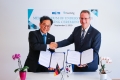
KETI가 독일 포츠담 프라운호퍼 IAP 연구소 컨퍼런스룸에서 프라운호퍼 IAP 연구소와 양자점 디스플레이 분야 기술개발을 위한 업무협력 MOU를 체결했다. IAP는 바이오폴리머, 기능성 폴리머 시스템, 합성 폴리머 기술, 생명과학·바이오 공정용 폴리머, 나노응용기술 등 7개 연구본부를 운영 중이다. 또 공정개발 및 최적화, 시험 분석 및 컨설팅 등의 기업지원 서비스를 제공, 민간 기업과 활발한 협력을 진행 중이다. KETI와 IAP는 2009년부터 디스플레이 분야 소재·소자 기술개발을 위해 공동기술개발, 연구 인력파견 등을 통해 협력을 이어오고 있다. 핵심 소재 및 소자구현 공정기술에 대한 공동연구를 통해 국내 기업의 디스플레이 산업 경쟁력 확보에도 기여하고 있다.
2019-09-10 오전 11:16:57by 이수민 기자

.png)

[열린보도원칙] 당 매체는 독자와 취재원 등 뉴스이용자의 권리 보장을 위해 반론이나 정정보도, 추후보도를 요청할 수 있는 창구를 열어두고 있음을 알려드립니다.
고충처리인 장은성 070-4699-5321 , news@e4ds.com