


Webinars
# 3 Major CAE Technology Application Methods to Accelerate PCB Thermal Design Optimization Work
| Session Preview | ||
|---|---|---|
| Session 1 | Dr. Park Jun (CTO) (VENG) |
- Abaqus Analysis for Defect Prediction in PCB Manufacturing Process and Proactive Design Response |
| Session 2 | Bae Jong-seon, CEO (Dassault Systèmes Korea) |
- Thermal and EMI/EMC Analysis of PCB Using CST |
As requirements and technologies for electrical and electronic products advance and become increasingly sophisticated, numerous errors and defects are occurring in the design and manufacturing processes. Consequently, the need for structural and electromagnetic analysis verification in conjunction with manufacturing processes from the design stage onwards is growing day by day.
Accordingly, this online seminar will share analysis (CAE) technologies for PCBs and electronic products equipped with PCBs, and through pre-verification, we will present methods to enhance reliability in product development and manufacturing stages while significantly reducing development timeframes.
1. PCB Warpage Simulation
PCBs are formed by sequentially laminating signal layers and dielectric layers, creating a multilayer structure consisting of as few as several to as many as dozens of layers depending on the product. A thermal process is essential to manufacture a completed PCB, and due to product characteristics, PCBs are inevitably exposed to heat generated by electrical properties during operation.
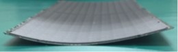
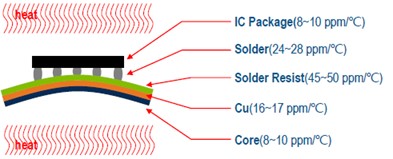
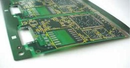
In such environments, PCBs may fail to maintain their original shape and become warped due to thermal imbalance. This phenomenon is collectively referred to as "warpage." While there are multiple factors causing warpage, such as environmental conditions in the manufacturing process, PCB design thickness and size, and copper foil patterns, the fundamental cause is that the coefficient of thermal expansion differs between layers.
 |
 |
 |
As PCB products have become miniaturized, higher-powered, and higher-density, it has become possible to commercialize lightweight products with lower power consumption. However, the increased heat density has raised the risk of warpage occurrence.
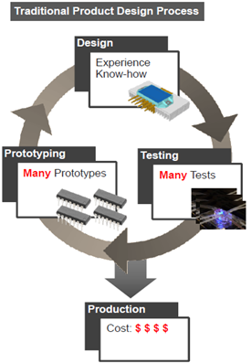
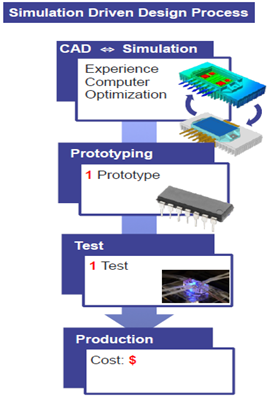
In past product development cycles, design was conducted based solely on engineer experience and know-how, and warpage defect verification and improvement were achieved through the production and testing of numerous prototypes.
This product development cycle requires significant cost and time investment, and has the disadvantage that improvement measures for defects must rely solely on engineer experience. To overcome this situation, product development processes based on analytical defect prediction have been implemented.
 |
 |
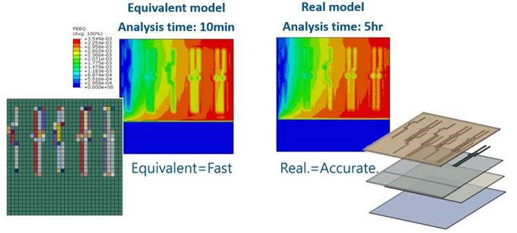
Analysis of warping phenomena primarily uses the finite element method. Analysis is performed using Abaqus, a nonlinear analysis tool provided by Simulia, Dassault Systèmes' simulation specialist brand. During the analysis preparation stage, finite element modeling of the PCB is necessary. However, due to the complexity of PCB structure, the Trace mapping technique is applied to reduce analysis time. This method divides the entire layout into several unit segments and establishes equivalent material properties by applying the volume ratio of each material existing within the respective unit segment.
For example, if a copper foil pattern exists at 50% and a dielectric exists at 50% in one layer, it is assumed that the layer has mixed characteristics of 50% copper material properties and 50% dielectric material properties. By applying thermal loads and mechanical constraints to the constructed finite element model, the deformation and stress state of PCB warpage can be obtained through nonlinear analysis. Regarding finite element model creation, it can be applied much more easily through the PCB Modeler Plug-in supplied by VENG.
2. Chip Placement Optimization
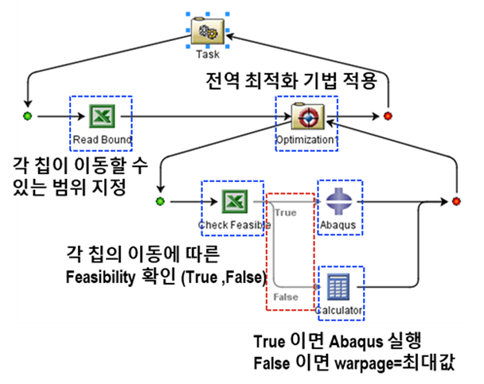
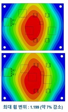
If chip placement can be altered to minimize warping, the placement can be optimized through Isight and Abaqus provided by Simulia. Through this optimization process, while PCB warping caused by thermal loads cannot be completely eliminated, a placement configuration can be found that minimizes its impact.
 |
 |
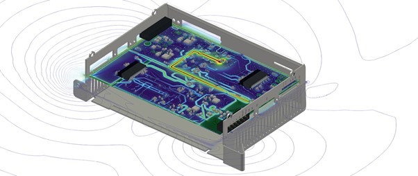
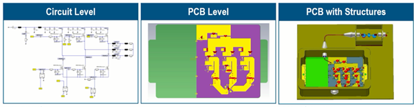
3. Thermal and EMC/EMI Analysis of Electronic Products and Automotive Electrical Components
With the advancement of electronic devices and automotive electrical equipment and increased PCB demand, the importance of thermal analysis and EMI/EMC analysis of PCBs is also growing. In this session, we aim to discuss thermal analysis and EMI/EMC simulation, which are major causes of defects in PCB development and PCBs in actual mounted applications.

Comments
- 43 Comments
- 신*일 (2021-04-01 오전 11:17:49)
- 좋은 세미나 감사드립니다.
- 남*연 (2021-03-25 오후 3:59:05)
- SoC가 올라간 SBC를 개발중인데 참고가 될것 같습니다. 감사합니다.
- 김*식 (2021-03-25 오전 11:44:59)
- EMC와 열문제는 고질적인 것 같아요. 자사 제품에 적용한 방법론 개발에 힘써보아야 겠습니다.
- 김*석 (2021-03-25 오전 11:35:06)
- 당첨되면 좋겠다!
- 박*직 (2021-03-25 오전 11:27:54)
- 고전력 제어 회로 설계시 아주 큰 도움이 되겠습니다.
- 김*화 (2021-03-25 오전 10:49:59)
- 요즘 온도 시험 스펙이 높아져 어려움을 겪고 있는데 좋은내용 시청하고 있습니다. 열심히 배우겠습니다. 감사합니다.
- 강*주 (2021-03-25 오전 10:39:08)
- 현재 산업 트렌드에 필요한 내용입니다. 경청 하도록 하겠습니다 감사합니다!
- 박*철 (2021-03-25 오전 10:25:25)
- 유익한 웨비나 감사합니다
- 김*환 (2021-03-25 오전 10:17:44)
- 유익한 웨비나가 될 듯 하네요
- 배*역 (2021-03-25 오전 10:05:28)
- 세미나 준비해 주셔서 감사합니다.