기사입력 2021.09.14 11:29
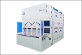
과학기술정보통신부 산하 한국기계연구원(원장 박상진)이 국내 최초로 400㎚(나노미터)급 레이저 직접 리소그래피 장비 국산화에 성공했다. 반도체 생산성을 획기적으로 개선할 수 있는 기술로 기대를 모은다.
2021-08-13 오후 1:56:16by 배종인 기자
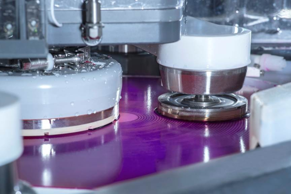
IC 제조 공정 중 3D NAND, DRAM, 고급 로직 공정에서 웨이퍼 에지 박리, 파티클, 잔여물로 인해 웨이퍼 에지 수율 저하가 발생하고 있다. 이를 해결하기 위해 전체 공정 수율 제고 필요성이 커지고 있다. ACM 리서치 베벨 에치 식각 장비는 습식 식각 방식을 사용해 웨이퍼 에지의 다양한 유전체, 금속 및 유기 물질 막질과 미립자 오염 물질을 제거한다.
2021-08-26 오후 2:16:07by 이수민 기자
SEMI는 최신 반도체 장비시장 통계 보고서를 통해 2분기 전 세계 반도체 장비 매출액이 지난해 같은 기간보다 48% 급증하여 분기 역대 최대 매출액인 249억 달러를 달성했다고 8일 발표했다. 이는 1분기 대비 5% 상승한 수치다.
2021-09-09 오전 8:42:33by 이수민 기자

[열린보도원칙] 당 매체는 독자와 취재원 등 뉴스이용자의 권리 보장을 위해 반론이나 정정보도, 추후보도를 요청할 수 있는 창구를 열어두고 있음을 알려드립니다.
고충처리인 장은성 070-4699-5321 , news@e4ds.com