코로나19 팬데믹으로 반도체 수요가 늘며 파운드리 매출도 늘고 있다. 1987년 설립된 TSMC는 고객의 제품을 위탁받아 제조하는 순수 파운드리 모델을 개척했다. 올 2분기엔 세계 파운드리 시장의 55%를 차지했고, 5나노 칩 매출 비중이 18%에 육박하는 등 매출과 기술 면에서 1위를 고수 중이다. 지난 8월에는 시가총액 기준으로 중국의 텐센트를 제치고 아시아 시가총액 1위 기업이 됐다.
TSMC, 파운드리 비즈니스 모델 최초 제시
반도체기업·아태지역기업 중 시가총액 1위
정부 지원·높은 경영 자유도·인재 집중 영향
반도체 업계는 인텔, 삼성전자처럼 반도체를 설계·제작·판매하는 ‘종합반도체회사(Integrated Device Manufacturer; IDM)’, 퀄컴, 엔비디아처럼 설계만 담당하고 생산을 위탁하는 ‘팹리스(Fabless)’, TSMC, UMC처럼 생산만 하고 설계는 하지 않는 ‘파운드리(Foundry)’, ASML, 램리서치 같은 장비공급업체로 구성된다.
파운드리는 반도체의 디자인을 전문으로 하는 팹리스 기업으로부터 제조를 위탁받아 반도체를 위탁생산하는 기업으로 대만의 TSMC, UMC, 미국의 글로벌 파운드리, 중국의 SMIC 등이 있다. IDM 일부는 자사 반도체뿐만 아니라 타 기업의 반도체를 생산하는 파운드리 기능을 수행한다. 삼성전자, SK하이닉스가 그렇다.
코로나19 팬데믹으로 반도체 수요가 늘며 파운드리 매출도 늘고 있다. 트렌드포스에 의하면, 세계 파운드리 시장은 2019년 600억 달러에서 2020년 682억 달러로 13.6% 증가했고, 2024년에는 944억 달러로 성장할 것으로 전망된다.
▲ TSMC, 반도체업계 시가총액 1위 기업 [사진=TSMC]
대만의 TSMC(Taiwan Semiconductor Manufacturing Company)는 세계 최초의 파운드리 업체로, 올 2분기 세계 파운드리 시장의 55%를 차지했고, 5나노(㎚) 칩 매출 비중이 18%에 육박하는 등 매출과 기술 면에서 1위를 고수 중이다.
한국전자통신연구원(ETRI) 전황수, 김현탁, 노태문 연구원은 ‘TSMC 반도체 기술 동향 및 성공요인 분석’ 보고서를 통해 파운드리 1위 기업이 어떻게 반도체 1위 기업으로 성장했는지를 짚어보고, 국내 반도체업계가 가야할 길을 제시했다.
◇ 세계 최초로 파운드리 비즈니스 모델 제시한 TSMC
1987년 설립된 TSMC는 대만 신주과학단지에 본사를 두고 있다. 고객의 제품을 위탁받아 제조하는 순수 파운드리 모델을 개척했는데, 자체 이름으로 반도체 제품을 설계, 제조 또는 판매하지 않기로 해 고객과 직접 경쟁하지 않는다.
1993년에 대만증권거래소(TWSE)에 상장됐고, 1997년에는 뉴욕증권거래소(NYSE)에 대만 기업으로서 처음으로 상장됐다. 1993년에는 대만 최초로 8인치 웨이퍼 팹을 건설했고, 2000년에는 미국 텍사스 인스트루먼트(TI)와 대만 에이서의 합작 기업인 ‘TI-에이서’ 반도체와 스다(世大) 반도체를 합병했다.
2000년 ‘팹 6’ 완공으로 12인치 웨이퍼를 생산하기 시작했고, 2003년에는 0.13㎛(마이크로미터) 공정을 가동해 지금까지 세계 파운드리 시장을 장악하고 있다.
TSMC는 2020년 실적으로 연결 매출 455억 1,000만 달러, 순이익 176억 달러를 달성하여 2019년보다 각각 31.4%와 57.5% 증가했다. 2021년 8월에는 시가총액 기준으로 중국의 텐센트를 제치고 아시아 시가총액 1위 기업이 됐다. 또한, 이미 2020년에 시가총액 6,700억 달러를 달성하며 세계 최고의 반도체기업이 됐다.
고객으로는 애플, 퀄컴, 미디어텍, 엔비디아, 브로드컴, AMD, 자일링스 등 팹리스 업체뿐만 아니라, TI, NXP, 인피니언, ST마이크로일렉트로닉스 등 반도체업체들의 제품을 위탁생산하는 등 세계 대다수 반도체업체를 고객으로 두고 있다.
◇ 7나노 이하 공정 비중 49% 육박 “3나노 검증 중”
TSMC는 510개 고객을 위해 272개 기술을 사용해 10,761개 제품을 생산한다. 지난해만 6,900개 특허를 등록했고, 12,000개의 기밀 노트를 교환했으며 5나노 기술을 상용화했다. 2020년 기준 연 1,300만 개의 300㎜ 상당 웨이퍼 생산 능력을 보유 중이며, 2마이크로에서 5나노의 노드를 가진 고객을 위한 칩을 생산한다.
6개의 12인치 웨이퍼 팹, 6개의 8인치 웨이퍼 팹, 1개의 6인치 웨이퍼 팹을 갖고 있다. 대다수 팹이 대만에 있고 100% 자회사인 중국 난징에 12인치 웨이퍼 팹, 상하이와 美 웨이퍼테크(WaferTech) 자회사에 8인치 웨이퍼 팹이 있다.
공정별로는 2021년 2분기 기준 7나노 이하 공정 비중이 49%에 달한다. 5나노가 18%, 7나노가 31%를 점유하고, 비교적 범용기술인 28나노가 11%, 40/45나노가 7%, 65나노가 5%, 90나노가 3%를 차지하고 있다. 지역별 비중으로는 북미 62%, 중국 17%, 일본 제외 아시아 11%, 유럽 5%, 아시아 5%이다. 용도별로는 스마트폰 48%, 고성능 컴퓨팅 33%, IoT 8%, 가전제품 4%, 자동차 3%, 기타 4%다.
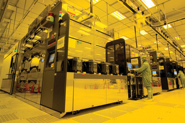
▲ 현재 TSMC는 애플과 인텔로 부터 3나노 칩 물량을
수주 받기 위해 분주한 상태다 [사진=TSMC]
TSMC는 5/7나노 생산 능력을 최초로 제공한 파운드리며, 극자외선(EUV) 리소그래피 기술을 대량으로 상용화했다. 지난해 6월 애플이 맥 컴퓨터 제품군을 Arm 기반 프로세서로 전환함에 따라 5나노 Arm 프로세서를 생산할 방침이다.
지난 7월, 애플과 인텔은 TSMC의 3나노 기술을 사용한 반도체 설계 검증을 하고 있다. 기존 5나노 대비 성능은 10~15% 향상되고, 전력을 25~30% 절감한다.
TSMC는 2021년에 설비투자에 300억 달러를 투자하고, 세계적인 반도체 공급난을 해소하고 각국 정부의 요청에 따라 2024년까지 3년간 총 1,000억 달러를 투자해 미국, 일본, 독일에 파운드리 공장을 설립할 계획이다.
◇ 삼성전자와 다르게 고객과 경쟁하지 않는 TSMC
TSMC는 “고객과 경쟁하지 않는다”를 모토로 고객이 맡긴 제품을 위탁생산하는 데 전념해 왔다. 1,000여 개의 반도체 관련 기업이 치열하게 경쟁하는 웨이퍼 설계 분야에서 설계도의 기밀 유지는 기업의 생사가 달린 일이다. 특급기밀이 담긴 설계도를 웨이퍼 파운드리 팹에 보내 생산하는 과정에서 기밀이 샐 우려가 크다.
TSMC는 기밀을 절대 준수하고, 성실한 관리로 고객에 대응했다. 일단 수주하면 손실이 나도 감수했고, 약속을 철저히 지켜 고객의 신뢰를 얻었다. 모리스 창 설립자는 고객과의 무경쟁 원칙이 TSMC 성공의 가장 큰 비결이라고 밝혔다. 그 말대로 GPU 분야의 엔비디아와 AMD, AP 분야의 퀄컴과 미디어텍, RF 분야의 브로드컴과 리얼텍이 자사의 제품을 TSMC에 안심하고 발주하고 있다.
애플의 ‘아이폰’이 휴대폰 시장을 뒤집은 이후, 가장 중요한 부품인 애플리케이션 프로세서(AP)는 그간 삼성전자가 독식했었다. 그러나 삼성전자 스마트폰의 세계 시장 점유율이 올라가면서 양사의 경쟁이 치열해지자 TSMC에게 새로운 기회가 찾아왔다. 모리스 창은 애플에 접근해 아이폰 AP의 생산을 타진했다.
삼성전자와 TSMC 간 미래 전개될 특허권 분쟁을 우려하여 애플과 TSMC는 ‘아이폰 5’에 사용할 ‘A6’ SoC 설계 문제부터 해결하고, TSMC는 2012년 8월까지 계속 IP를 애플에 넘겨 검증을 받는 과정을 통해 그 위험을 최소화했다.
▲ 애플은 아이폰 6부터 최근 발표한 아이폰 13까지
자사 휴대폰에 TSMC 생산 AP를 탑재하고 있다 [사진=애플]
2013년 4월, 애플은 TSMC와 ‘A7’ SoC 기밀 데이터를 공유했고, TSMC는 2014년부터 ‘A8’ SoC 생산을 시작, 현재 ‘M1 및 A15 바이오닉’ 등을 생산 중이다.
◇ 높은 영업이익, R&D 비용으로 반 수가량 재투자
TSMC의 영업이익률은 평균 30~40%로, 기술 개발과 설비투자에 재투자한다. 2020년 설비투자액은 181억 달러로, 매출액 477억 달러의 38%를 투자했다. 연구개발비는 2010년 9억 4,300만 달러에서 2020년 37억 2,000만 달러로 늘었고, 연구개발 인력도 2010년의 2,881명에서 2020년 7,404명으로 3배나 증가했다.
2001년 이후 12인치 웨이퍼 팹을 20년간 5개, 평균 4년에 1개씩 건설했다. 2000년에는 세계 최대의 반도체 공장인 팹 6을 준공했다. 2003년, TSMC는 0.13마이크로미터 기술을 개발해 인텔, 삼성전자와 함께 세계 3대 반도체기업에 진입했다. 2008년 미국발 금융위기로 인해 전 세계 반도체기업들이 투자를 줄일 때 TSMC만 설비투자를 크게 늘렸고. 2009년부터 매년 100억 달러를 투자했다.
반도체는 나노 단위인 회로의 선폭이 좁을수록 저전력 고효율 칩을 만들 수 있다. 반도체 성능을 좌우하는 나노미터 단위 미세공정 시장 선점을 위해 TSMC와 삼성전자가 기술 개발과 설비 확충 경쟁을 벌이고 있다. 미세공정에 적용하는 스마트폰 AP, PC용 CPU 등은 주문 물량이 많고 영업이익률이 높기 때문이다.
TSMC는 2000년대 초 블루팀과 레드팀이라는 R&D 조직을 만든 후 블루팀에는 16나노→7나노→3나노, 레드팀에는 20나노→10나노→5나노 공정 개발을 목표로 주고 내부 경쟁을 시켰다. 2018년 7나노 제품 양산에 들어갔고, 2020년에는 5나노 양산을 시작했다. 2022년 하반기에 3나노 제품 양산에 돌입할 전망이다.
◇ 대만 정부, 가장 강력한 TSMC 우군
대만 정부는 1987년, 모리스 창이 TSMC를 설립할 때부터 적극적으로 후원했다. TSMC는 대만공업기술연구원(ITRI)에서 분사(Spin-off)한 기업으로, ITRI 원천기술이 TSMC로 이전됐다. 대만 행정원은 초기 TSMC 지분 48.3%를 보유했고, 1993년 TSMC 민영화 이후에도 국가개발기금을 통해 6.4%를 소유하고 있다.
TSMC 임직원은 이사회에 의해 고용돼나 대주주는 이사회를 통제할 수단이 없다. 이사회는 실적에 따라 임직원의 보수와 연임을 결정하며, 임직원은 자신의 이익을 챙길 수 없다. 따라서 주주 눈치를 보지 않는 막대한 투자가 가능하다.
또한, TSMC 본사와 주요 팹이 위치한 신주과학단지(新竹科學工業圓區)는 대만의 대표적인 IT 산업 클러스터로, 입주 기업들은 5~9년간 법인세 면제, 낮은 대출금리, R&D 보조금 등 각종 혜택을 받는다. 거기다 대만 정부는 팹 건설에 필요한 막대한 용수와 전기 인프라도 구축했다. 대만 각지를 하루 만에 이동할 수 있는 고속철도와 고속도로 인프라도 TSMC 성공에 크게 기여했다.
대만에선 여러 산업 중 반도체산업의 연봉이 가장 높아 인재가 많이 몰리고 있다. TSMC는 정부 차원의 장학혜택과 산학연계 교육모델에 기반해 우수 인력을 유치하고 있다. 특히, ‘주식 보너스 제도’로 순수익의 10%를 신주로 발행하고 액면가로 직원들에게 나눠주었는데 대만 정부는 시세차익에 세금을 면제해줬다.
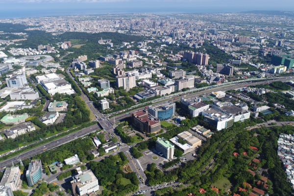
▲대만 반도체산업의 본산인 신주과학단지 전경
[사진=대만 과학기술부]
신주과학단지에는 TSMC 외에 UMC, 미디어텍, 노바텍, 리얼텍 등의 주요 반도체업체들이 포진해있다. 이들은 칩 설계 회로와 제조 공정의 구현, 각종 IP에 얽혀 있어 오랜 기간 협력해왔고, 숙련된 고급 기능 인력을 다량 배출하고 있다. 정부 지원과 높은 경영 자유도, 인재 집중 등이 TSMC 성공의 밑거름이다.
◇ TSMC 성장이 韓 반도체산업에 던지는 시사점
팬데믹으로 촉발된 반도체 부족 사태는 당분간 계속될 전망이고, 이를 근본적으로 해결하기 위해서는 파운드리 시설을 확대해야 한다. 파운드리에서 생산하는 시스템 반도체는 다품종 소량생산으로 생산을 늘리는데 고객사의 안정적인 수요 확보, 막대한 시설 투자, 3년 이상의 시간이 소요되므로 증설이 쉽지 않다.
더불어 파운드리는 고가 장비와 숙련된 엔지니어의 노하우를 조합하는 것이 핵심이다. 불량률을 낮추기 위해 24시간 내내 몰입해야 하고, 미세화로 공정 수는 더욱 늘어났다. 로직 칩을 완성하려면 복잡한 개별 공정을 수없이 거쳐야 한다.
국내 파운드리 업계는 세계 2위의 삼성전자, 세계 10위의 DB하이텍을 제외하고는 대다수가 규모가 작고 기술력이 취약하다. 고객인 팹리스가 매우 영세해 안정적인 수요기반도 없다. 국내 반도체산업은 대만보다 국제 경쟁력이 크게 떨어진다.
파운드리 산업이 발전하기 위해서는 유능한 인재를 확보해야 한다. 인력 부족을 해결하기 위해 학과 증원, 현장 경험이 많은 교수진 충원, 산업체 계약학과 신설, 대학 반도체 연구센터 증설이 필요하다. 또한, 대만처럼 세제 혜택, 전력 및 용수 공급 등 인프라 제공, 관련 법 마련 등 정부 지원이 뒷받침되어야 한다. 장기적으로 팹리스 등 수요 업체와 파운드리 간 협력 네트워크를 구축해야 할 것이다.
.jpg)

.jpg)