10년 전 세계 파운드리 시장 점유율에서 약 1%에 불과하던 삼성이 지금은 파운드리 1위 TSMC의 아성에 도전할 만큼 격차를 좁혔다. 삼성전자 파운드리사업부 출범 5년 만에 차세대 GAA 기반 3나노 공정을 세계 최초로 선보이며 공정 미세화에서 TSMC보다 한 발 이상 빠른 행보를 보여주고 있다.
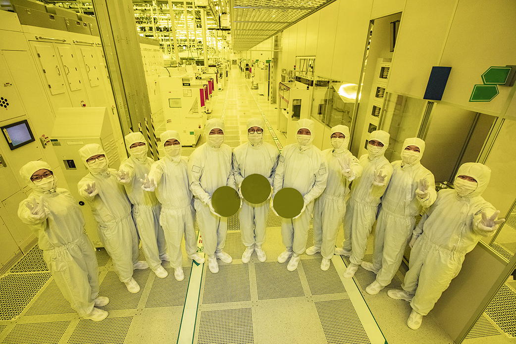
▲3나노 파운드리 양산에 참여한 파운드리사업부, 반도체연구소, 글로벌 제조&인프라총괄 주역들이 손가락으로 3을 가리키며 3나노 파운드리 양산을 축하하는 모습 (사진 - 삼성전자)
Gate-All-Around(GAA) 차세대 트랜지스터 기술 최초 상용화
3나노 1세대, 5나노 대비 전력 45%↑·면적 16%↓·성능 23%↑
10년 전 세계 파운드리 점유율에서 1%에 불과하던 삼성이 지금은 파운드리 1위 TSMC의 아성에 도전할 만큼 기술 격차를 좁혔다. 삼성전자 파운드리사업부 출범 5년 만에 차세대 GAA 기반 3나노 공정을 세계 최초로 선보이며 공정 미세화에서 TSMC보다 한 발 이상 빠른 행보를 보여주고 있다.
삼성전자가 세계 최초로 GAA(Gate-All-Around) 기술을 적용한 3나노(nm, 나노미터) 파운드리 공정 기반의 초도 양산을 시작했다고 30일 밝혔다.
3나노 공정은 반도체 제조 공정 가운데 가장 앞선 기술이며, 차세대 트랜지스터 구조인 GAA 신기술을 적용한 3나노 공정 파운드리 서비스를 삼성전자가 세계 최초로 선보인 것이다.
삼성전자의 3나노 GAA 1세대 공정은 기존 5나노 핀펫(FinFET) 공정과 비교해 △전력 45% 절감 △성능 23% 향상 △면적 16% 축소를 실현했다.
이에 그치지 않고 삼성측은 GAA 2세대 공정도 2023년 양산을 목표로 개발과 테스트 중에 있다고 밝혔다. GAA 2세대는 △50% 전력 절감 △30% 성능 향상 △35% 면적 축소의 성능 발전이 이뤄질 전망이다.
삼성전자는 3나노 공정의 고성능 컴퓨팅(HPC)용 시스템 반도체를 초도 생산한 데 이어, 모바일 SoC 등으로 확대해 나갈 예정이라고 설명했다.
최시영 삼성전자 파운드리사업부장(사장)은 "삼성전자는 파운드리 업계 최초로 '하이-케이 메탈 게이트(High-K Metal Gate)', 핀펫, EUV 등 신기술을 선제적으로 도입하며 빠르게 성장해 왔고, 이번에 MBCFET GAA기술을 적용한 3나노 공정의 파운드리 서비스 또한 세계 최초로 제공하게 됐다"며, "앞으로도 차별화된 기술을 적극 개발하고, 공정 성숙도를 빠르게 높이는 시스템을 구축해 나가겠다"고 밝혔다.
■ 삼성표 최첨단 MBCFET GAA 독자 기술
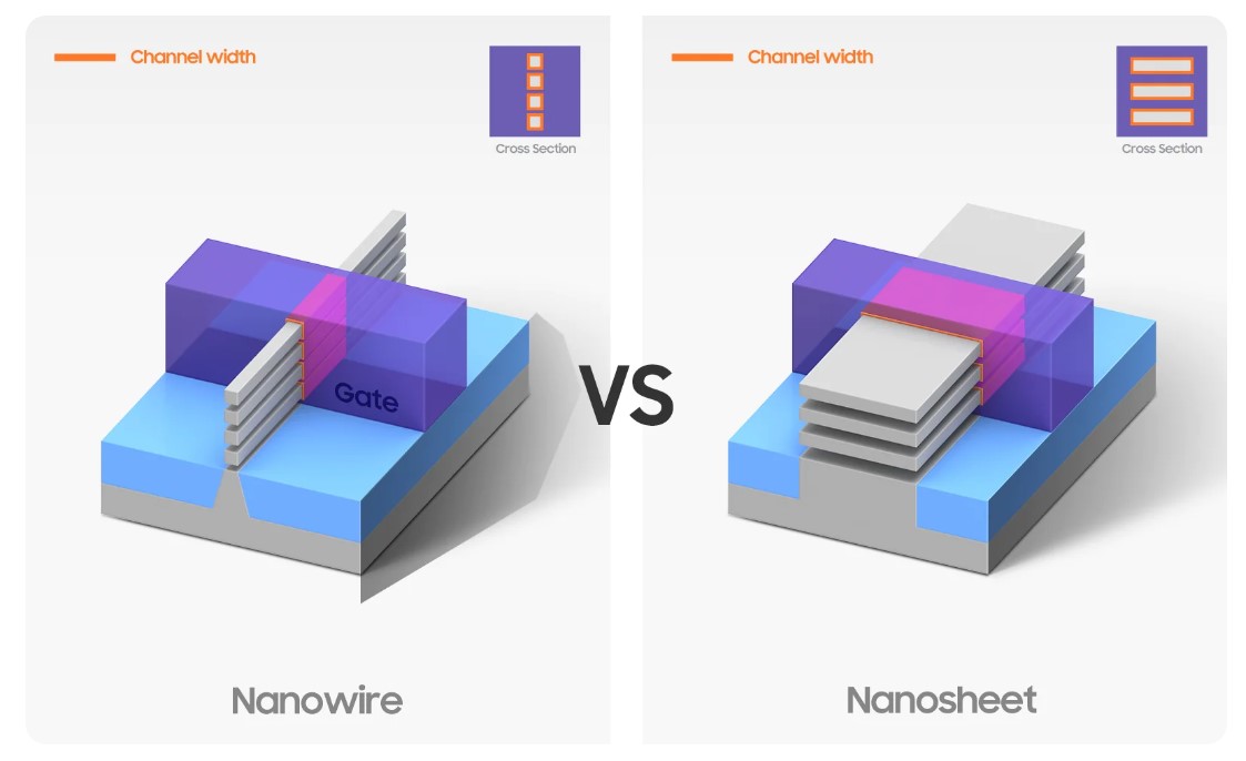 ▲나노와이어와 나노시트 구조 비교 (이미지-삼성뉴스룸)
삼성전자는 이번에 반도체를 구성하는 트랜지스터에서 전류가 흐르는 채널의 4개 면을 게이트(Gate)가 둘러싸는 형태인 차세대 GAA 기술을 세계 최초로 적용했다.
채널의 3개 면을 감싸는 기존 핀펫 구조와 달리, GAA 기술은 게이트의 면적이 넓어지며 공정 미세화에 따른 트랜지스터 성능 저하를 극복하고 데이터 처리 속도와 전력 효율을 높이는 차세대 반도체 핵심 기술로 손꼽힌다.
여기에 더해 삼성전자는 채널을 얇고 넓은 모양의 나노시트(Nanosheet) 형태로 구현한 독자적 MBCFET GAA 구조도 적용했다.
나노시트의 폭을 조정하면서 채널의 크기도 다양하게 변경할 수 있다. 기존 FinFET 구조는 게이트를 감싼 Fin의 높이를 조절할 수 없기에 수평 방향으로 핀 개수를 증가시켜 채널 크기를 늘릴 수 있었다. 이는 볼연속적인 채널 크기의 조정만 가능했는데 이번에 양산되는 3나노에 적용된 MBCFET 기술은 나노시트 구조이기에 시트 폭 증감이 유연해 이를 통한 다양한 채널 크기가 가능한 것이다.
또한 기존 핀펫 구조나 일반적인 나노와이어(Nanowire) GAA 구조에 비해 전류를 더 세밀하게 조절할 수 있어 고성능·저전력 반도체 설계에 큰 장점이 있다. 이는 4면을 채널로 하는 구조를 통해 On-Off 특성을 향상시켰으며 이를 통해 비유하자면 수도꼭지 기능이 좋아져 살짝만 잠가도 물이 새지 않는 것처럼, 낮은 전압에도 트랜지스터가 알맞게 동작해 구동 전압은 낮추고 전력 효율은 높이는 결과를 가져왔다.
■ 설계 공정 기술 최적화를 통한 극대화된 PPA 구현
.jpg) ▲삼성전자 화성 캠퍼스 (사진-삼성전자)
▲삼성전자 화성 캠퍼스 (사진-삼성전자)
삼성전자는 나노시트 GAA 구조 적용과 함께 3나노 설계 공정 기술 공동 최적화(DTCO, Design Technology Co-Optimization)를 통해 PPA(Power:소비전력, Performance:성능, Area:면적)를 극대화하는 데 노력을 기울여왔다.
삼성전자 3나노 GAA 1세대 공정은 기존 5나노 핀펫 공정과 비교해 △전력 45% 절감 △성능 23% 향상 △면적 16% 축소를 이뤄냈으며 내년도 양산 예정인 GAA 2세대는 △전력 50% 절감 △성능 30% 향상 △면적 35% 축소의 발전이 있을 것으로 보인다.
삼성전자는 “앞으로 고객 요구에 최적화된 PPA, 극대화된 전성비(단위 전력당 성능)를 제공하며, 차세대 파운드리 서비스 시장을 주도해 나갈 계획”이라고 밝혔다.
삼성전자는 시높시스, 케이던스 등 SAFE(Samsung Advanced Foundry Ecosystem) 파트너들과 함께 3나노 공정 기반의 반도체 설계 인프라 및 서비스를 제공함으로써, 3나노 반도체 생태계를 확장해 나가고 있다.
상카 크리슈나무티 시높시스 실리콘 리얼라이제이션그룹 총괄 매니저는 “삼성전자와의 GAA기반 3나노 협력은 향후 △시높시스의 디지털 디자인 △아날로그 디자인 △IP 제품으로 계속 확장해 주요 고성능 컴퓨팅 어플리케이션을 위한 차별화된 SoC를 제공할 것이다”고 말했다.
톰 베클리 케이던스 Custom IC&PCB 그룹 부사장 겸 총괄 매니저는 “케이던스는 삼성전자와 협력해 자동화된 레이아웃으로 회로 설계와 시뮬레이션에서 생산성을 높일 수 있는 서비스를 제공한다”고 언급했다.
.jpg)
.jpg)