[전자파학회 하계학술대회]2.5·3D 반도체 미래, “전력·신호 무결성 必”
기사입력 2022.08.25 16:00
▲2022년 한국전자파학회 하계종합학술대회
전력·신호 무결성, "흠결 없는 것 아닌 영향 최소화 관건"
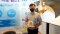
문성욱 삼성전자 마스터, "2.5D·3D 영역 크게 증가할 것"
문성욱 삼성전자 마스터, "2.5D·3D 영역 크게 증가할 것"
전세계 인구는 77억명가량되지만 사용하고 있는 디바이스의 숫자는 5,000억개가 넘는다. 반도체 트렌드는 1인당 PC, 휴대전화 보급율이 미미하던 2000년대 이전과 달리 시스코 글로벌 클라우드 인덱스 자료에 따르면 2008년을 기점으로 디바이스는 수는 인구 수를 넘어서고 1인당 평균 디바이스 보유량은 15개로 추산되며 2030년에는 1조2,500억개의 디바이스 수를 전망하기에 이른다.
반도체 트렌드는 무어의 법칙에 의거해 2년 주기로 2배 성능 발전을 이룩한 가운데 기술적 한계에 봉착하며 비용 문제와 미세공정 한계 등 혁신 장벽에 부딪혔다. 이에 차세대 기술 개발을 위한 다양한 발전 방안이 모색되고 있는 시점이다.
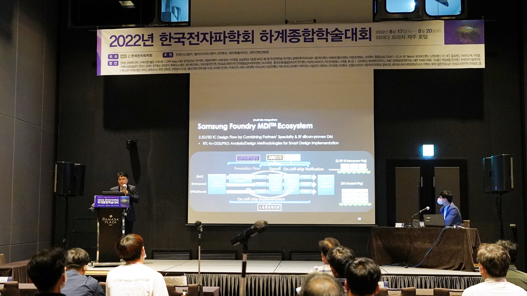
한국전자파학회 하계학술대회서 ‘2.5D·3D 반도체 설계 구현을 위한 Power&Signal Integrity 기술의챌린지’로 문성욱 삼성전자 파운드리사업부 마스터가 주제강연을 진행했다. 이날 삼성의 패키징 기술력과 전력 및 신호 무결성 해결과제에 대한 심도 있는 발표가 진행되자 참관객들의 발길이 이어졌다.
■ 이종집적 패키징 트렌드, 전력·신호 무결성(Integrity) 必
반도체 이종집적화(Heterogeneous Integration)의 등장 배경 중 하나는 비용 문제이다. 여러 칩렛(Chiplet)을 빌딩블록으로 조합해 단일 프로세서로 제작함으로써 수율은 높이고 비용은 낮출 수 있어 여러 반도체 제조기업에서 이를 채택했다.
첨단 노드 공정일수록 단가가 높고 수율이 낮기 때문에 다이가 클수록 불량이 발생할 가능성이 크며, 이에 따른 손실도 크다. 그렇기에 필요한 칩렛만을 첨단 노드 공정에서 설계해 다이 크기를 최소화하는 빌딩 블록 방식의 이종집적 패키징이야말로 수율과 성능 두 가지를 모두 만족시킬 수 있는 것이다.
“도덕적으로 무결성은 흠결이 없는 것이지만 반도체 설계에서 무결성은 흠결이 없는 상황이 아니라 흠이 있더라도 전력·신호에 영향을 주지 않게 설계하는 것이 실제적인 정의이다”
문성욱 마스터는 반도체 전력·신호 무결성을 정의하며 이는 미세한 부분까지 세심하게 설계해야 하는 분야임을 강조했다.
무결성은 △시스템 간 △트랜지스터 간 △모듈 간 등 다양하고 복합적으로 살펴봐야 하며 전력 측면에서 이슈는 △전압 강하(Voltage Drop) △스위칭 노이즈 △크로스토크가 있으며, 신호 측면에서는 △감쇠 특성 △전파 반사 △분산 △간섭 △크로스토크 등의 이슈가 존재한다.
■ 2.5D·3D 반도체의 과제와 미래
문성욱 마스터는 2.5D 실리콘 인터포저(Interposer)를 언급하며 “몇 해 전만 해도 다이 사이즈를 떠올리면 1000mm²(제곱밀리미터)까지가 한계였는데 최근에는 HBM도 8개 혹은 12개까지 들어가기 시작하면서 미래에는 2400mm² 또는 3200mm²를 준비해야 될 정도로 대형화되고 있다”고 말했다. 이에 데이터센터에서는 킬로와트급 파워가 요구되고 있다.
이러한 파워 문제로 인해 ‘디캡(디커플링 커패시터, Decoupling Capacitor)’ 솔루션을 적용한 설계구현에 초점을 맞추게 되며, 더불어 발열 문제를 해결하는 것이 패키징 엔지니어들이 많이 고민하는 지점이라고 문 마스터는 덧붙였다.
고성능 컴퓨팅(HPC)에서 기술적 난제는 △고성능 구현을 위해 다이 크기 증가 및 TAT(Turn Around Time) 감소 △높은 열밀도(Thermal Density) △다이 크기 증가에 따른 수율 문제와 빠른 수율 증가 △테스트 프로세스 증가에 따른 넓은 커버리지와 짧은 TAT 요구 △멀티 다이 PSI 분석 등이 있으며 향후 해결 과제로 남아 있다.
3D 집적회로(IC)는 HPC와 모바일 모두에서 활용이 가능하며 비용 절약적인 이점이 있다. 3D IC는 성능과 폼 펙터 측면에서도 이점을 가질 수 있다. 더불어 기술적 난제 또한 굉장히 많다는 문 마스터는 3D 반도체에서 기술적 난제를 둘러싼 부분은 바로 TSV(Through Silicon Via)라고 지적했다.
삼성 파운드리는 MDI(Multi Die Integration) 패키징을 위한 생태계 조성에 리더십을 발휘하고 있다. 시높시스, 지멘스, 앤시스 등과 같은 EDA 기업들과 함께 관련 툴을 개발한다. △시높시스와는 초기단계 노이즈 예방 PSI 디자인 솔루션 △앤시스와 Large DB 용량 PI·SI 솔루션 △물리적 검증과 Thermal/Stress 솔루션을 지멘스와 협업하고 있다. 문 마스터는 “2.5D·3D 패키징 영역이 글로벌 산업 전반에 대중적이지 않다 보니 EDA산업에서 툴이 빠르게 발전하진 않는 것”으로 진단했다.
문 마스터는 “반도체 트렌드는 2.5D·3D 영역이 크게 증가할 것으로 전망한다”며 “이에 대한 인프라 고민이 현존한 가운데 많은 준비가 필요할 것”으로 내다봤다. 삼성전자는 2.5D·3D 영역 확대에 따른 준비를 앞서 진행하고 있으며 일부 고객을 통해 이미 실현해 나가고 있다고 강조했다.
관련뉴스
-
[전자파학회 하계학술대회]6G·자율주행·우주·국방·EMI 전파 총망라
전자파 분야는 통신·위성뿐 아니라 전기차, 자율주행, 우주·항공, 국방, 의료, AI 등 다양한 응용 및 융합 분야로 확대되고 있으며 차세대 핵심 원천 기술의 근간이 되는 학문이다. 관련 아젠다를 주도하는 한국전자파학회가 하계종합학술대회를 개최하며 산학연을 총망라한 학문 교류의 장을 마련해 최근 성료했다.
2022-08-22 오후 2:32:39by 권신혁 기자
-
[전자파학회 하계학술대회]전기차 무선 충전, FOD·P2PS 연구 활발
전력 송신부와 수신부가 떨어져 있는 전기차 무선 충전 시스템에서 일어날 수 있는 사고 예방과 충전 효율을 높이기 위해서 FOD와 P2PS 기술 연구가 활발하게 이루어지고 있다.
2022-08-22 오후 4:40:31by 성유창 기자
-
[전자파학회 하계학술대회]웨이비스, “국내 유일 GaN 반도체 팹 보유”
차세대 반도체 소자로 손꼽히는 갈륨 나이트라이드(GaN) 반도체는 저전력 솔루션의 핵심으로 전력 효율이 높고 더 높은 주파수, 전압, 온도에서 낮은 전력 손실로 작동이 가능해 관련 시장이 점차 확대되고 있는 추세이다.
2022-08-23 오전 8:27:52by 권신혁 기자
-
[전자파학회 하계학술대회]센서뷰, “RF엔지니어 퍼포먼스 높이는 파트너”
5G·6G 차세대 통신 발전이 예고되며 전자기파 솔루션에 대한 시장의 니즈가 커지고 있다. 커넥티드카, 사물인터넷(IoT), 스마트 팩토리·시티 등 통신 기술 기반 서비스와 제품이 급격히 증가하는 가운데 5G 인프라와 와이리스 디바이스 솔루션을 갖춘 기술력 있는 10년 미만의 신생 기업들이 기술력을 앞세우며 경쟁에 나서고 있다.
2022-08-24 오전 9:11:01by 권신혁 기자

.jpg)
많이 본 뉴스
[열린보도원칙] 당 매체는 독자와 취재원 등 뉴스이용자의 권리 보장을 위해 반론이나 정정보도, 추후보도를 요청할 수 있는 창구를 열어두고 있음을 알려드립니다.
고충처리인 장은성 070-4699-5321 , news@e4ds.com