[권신혁의 혁신포커스] “반도체 미세화 한계, FD-SOI로 대응”
기사입력 2022.11.03 17:14
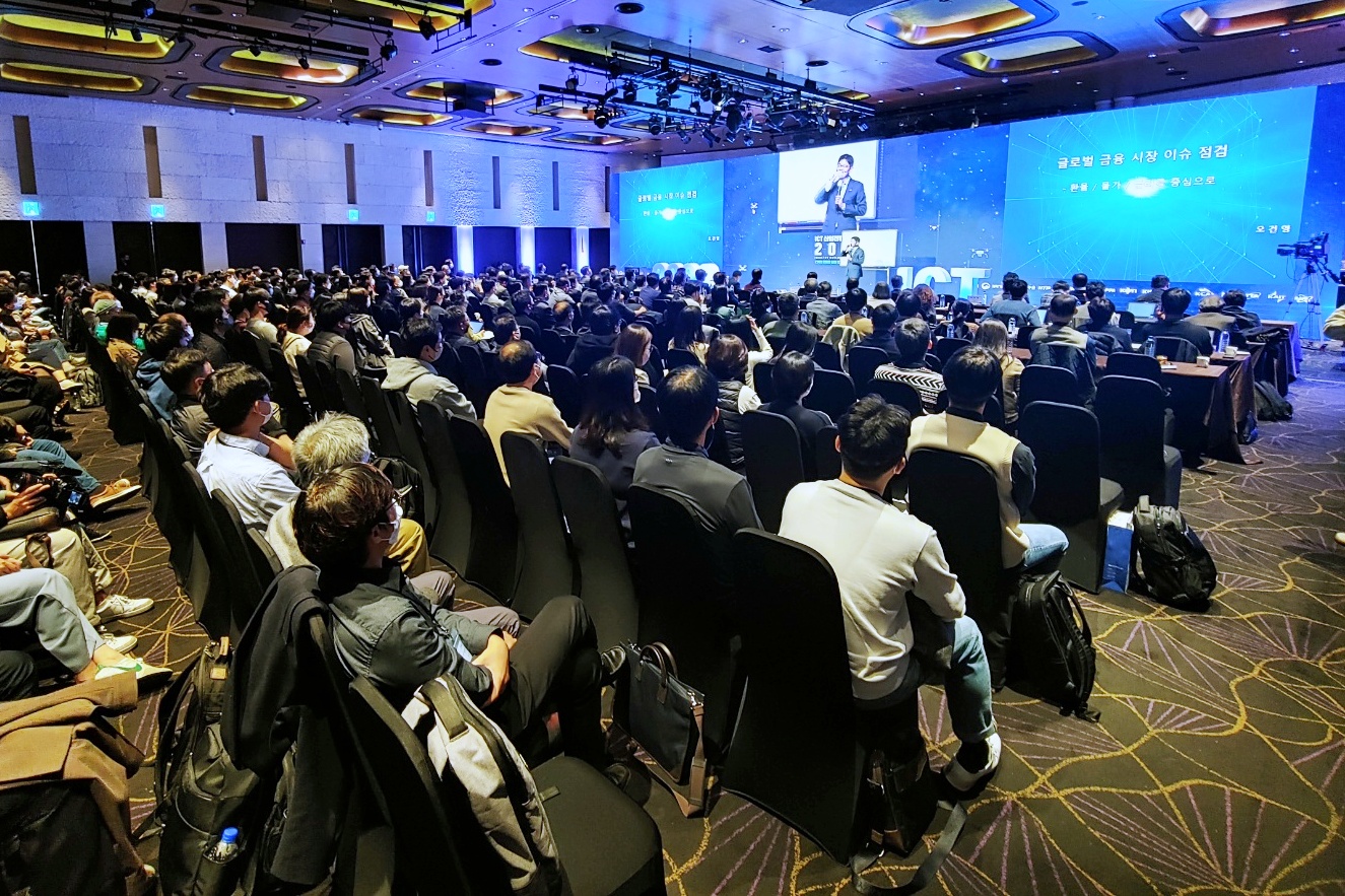
▲ICT산업전망컨퍼런스
프랑스국립과학연구원, “혁신 소자 가능 有”
FD-SOI기술, ST마이크로일렉트로닉스 주도
ICT산업전망컨퍼런스, 미래 대응방안 모색
FD-SOI기술, ST마이크로일렉트로닉스 주도
ICT산업전망컨퍼런스, 미래 대응방안 모색
반도체 미세화 한계 봉착으로 차세대 소자 및 기술 혁신에 대한 요구가 꿈틀대고 있다. ICT산업을 둘러싼 변화의 파도가 거센 가운데 반도체 공정이 미세화 될수록 기하급수적으로 높아지는 비용과 물리적인 한계에 대한 대안으로 FD-SOI 공정이 제시됐다.
국내외 ICT전망을 통해 미래 ICT산업 대응방안을 모색하는 ICT산업전망컨퍼런스가 서울 양재동 엘타워에서 3일 개최했다.
양일간 진행되는 이번 행사는 과학기술정보통신부가 주최해 ‘디지털 대전환을 넘어 디지털 대도약 시대로’를 주제로 △반도체 △모빌리티 △AI △경제 전망 △미래도시 등 다양한 주제의 세션을 준비해 온·오프라인으로 공개했다.
컨퍼런스의 첫 세션을 연 것은 소린 크리스톨로베아누 프랑스국립과학연구원 이사의 ‘반도체 패권의 도전’ 발표였다. 그는 FD-SOI 기술에 상당히 낙관적인 전망을 드러냈다.
반도체 미세화의 한계로 3나노미터 이하로는 한계에 봉착할 것이라는 소린 이사는 “이는 양자 터널링 현상 때문으로 반도체 미세화에서 성능 및 비용 등을 고려하면 10나노가 한계”라고 지적했다.
트랜지스터가 최소 크기에 곧 도달할 것을 전망한 가운데 실리콘 소자가 반도체 공정의 주류 소재임에 분명하고 향후 수십년간은 지배적 자리를 유지할 것이라고 밝히기도 했다. 그럼에도 그는 SOI 기술이 궁극적으론 혁신적인 소자 개발에 적용될 수 있다고 강조했다.
FD-SOI는 벌크 CMOS 대비 생산성에 있어서 가격 경쟁력이 뛰어나다. 또한 기생커패시턴스를 낮추고 누설전류도 감소시키며 초저전력은 물론 RF 커넥티비티와 밀리미터파 보안 등에 통합될 수 있다.
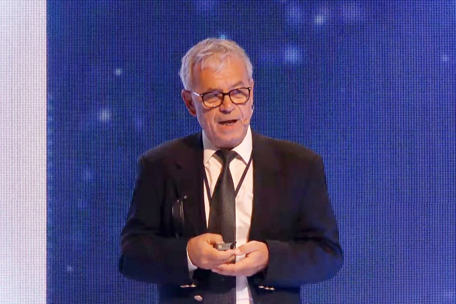
▲소린 크리스톨로베아누 프랑스국립과학연구원 이사
소린 이사는 FD-SOI 기술이 △커패시터리스 D램 △포토닉스 △3D 집적 △퀀텀 디바이스 △4게이트 트랜지스터 △인공 스파이크 뉴런 등에 적용 가능하다고 언급했다. 이외에도 그는 △무접합(Junctionless) 모스 트랜지스터 △적층형 나노와이어 및 나노시트 등의 적용 가능성을 덧붙였다.
이러한 FD-SOI는 ST마이크로일렉트로닉스사가 기술을 주도하고 있다. 최근 7월 ST는 프랑스 크롤에 기존 12인치 파운드리를 확장을 준비하며 FD-SOI 기반 기술 지원을 확대할 것이라고 밝혔다.
이날 컨퍼런스에는 △이재호 SK에너지 부사장 △오건영 신한은행 부부장 △유현준 대표건축가 △임진국 정보통신기획평가원 단장 등이 참여해 미래 전망을 밝히는 발표들을 진행했다.
전성배 정보통신기획평가원 원장은 개회사에서 “직면한 변화를 빠르게 파악하고 선제적으로 대비하는 것이 지속적인 성장과 혁신을 이뤄나갈 수 있는 방법”이라며 “위기 속 기회를 모색해 2023년을 준비하는 시간이 되길 바란다”고 말했다.
한편, 오는 2일차 행사에서는 △AI반도체 △지정학적 이슈 △메타버스·NFT △디지털 미디어 △양자 △차세대 통신 △인공지능 △사이버 보안을 주제로 세션이 진행된다.

관련뉴스
-
세계 100대 ICT 기업, 韓 단 2社
한국이 ICT 강국이라는 타이틀과 달리, 세계 100대 ICT 기업 중 한국 기업은 단 2개에 불과해 중국, 일본, 인도, 대만 등 ICT 경쟁국에 모두 뒤처지며, 소프트웨어, 팹리스 등 경쟁력이 낮은 우리나라 ICT 현실이 적나라하게 드러났다.
2022-07-12 오후 4:26:35by 배종인 기자
-
.jpg)
"디지털 생산성 강화 必"
화웨이는 글로벌 ICT 산업 분야 연례행사인 ‘화웨이 커넥트 2022(Huawei Connect 2022)’를 19일 방콕에서 개최했다. 켄 후 순환 회장은 “디지털화는 분명히 옳은 선택”이라며 “수요와 기술 모두 디지털화에 달렸다. 세계는 디지털 생산성을 촉발시키고 있으며, 이는 지금도 일어나고 있다”고 말했다.
2022-09-20 오전 8:13:52by 권신혁 기자
-
.png)
9월 ICT 수출 208.6억불…3개월 만에 200억불 회복
과학기술정보통신부는 2022년 9월 ICT 수출이 전년 동월 대비 4.5 % 감소했지만, 208.6억불을 달성했고, 무역수지는 79.4억불 흑자를 달성했다고 밝혔다.
2022-10-18 오전 10:49:21by 김예지 기자

.png)
관련 웨비나


많이 본 뉴스
[열린보도원칙] 당 매체는 독자와 취재원 등 뉴스이용자의 권리 보장을 위해 반론이나 정정보도, 추후보도를 요청할 수 있는 창구를 열어두고 있음을 알려드립니다.
고충처리인 장은성 070-4699-5321 , news@e4ds.com