[기술기고]Gerald Deboy, 인피니언-언제 실리콘에서 와이드 밴드갭으로 이전할 것인가
기사입력 2023.01.16 11:31
WBG, 총 유지비 구입비용 상쇄 고려 必
구입시 비싸지만 수명전반 비용 절감 장점
각각 활용사례 달라, 가격 상쇄기간 따져야
구입시 비싸지만 수명전반 비용 절감 장점
각각 활용사례 달라, 가격 상쇄기간 따져야
■ WBG, 더 높은 스위칭 주파수·전력 밀도에 개발자 채택 증가
MOSFET이나 IGBT 같은 실리콘 전력 디바이스는 오랜 기간에 걸쳐서 전력 애플리케이션에서 신뢰하게 동작하는 것으로 검증되었다. 가격대가 낮고, 시장에 다양한 제품이 출시되어 있으므로 디자이너들의 선택폭이 넓다. 또한 전력 엔지니어들이 오랜 기간 사용해 오면서 축적된 경험이 많고 친숙한 기술이다.
그래서 실리콘 디바이스가 다양한 용도로 널리 사용되고 있는데, 최근 들어서는 SiC나 GaN 같은 와이드 밴드갭(WBG) 디바이스로 눈을 돌리는 설계 엔지니어들이 늘고 있다. 와이드 밴드갭 디바이스는 실리콘보다 더 높은 스위칭 주파수로 동작할 수 있고, 더 높은 효율을 달성하고, 더 높은 전력 밀도를 가능하게 한다. 그러므로 전원장치의 크기를 줄이고 무게를 가볍게 할 수 있다. 또 다르게는 주어진 폼팩터로 출력 전력을 높일 수 있다.
그림 1은 전원장치에 있어서 Si, SiC, GaN 디바이스를 사용하기에 적합한 애플리케이션들을 보여준다.
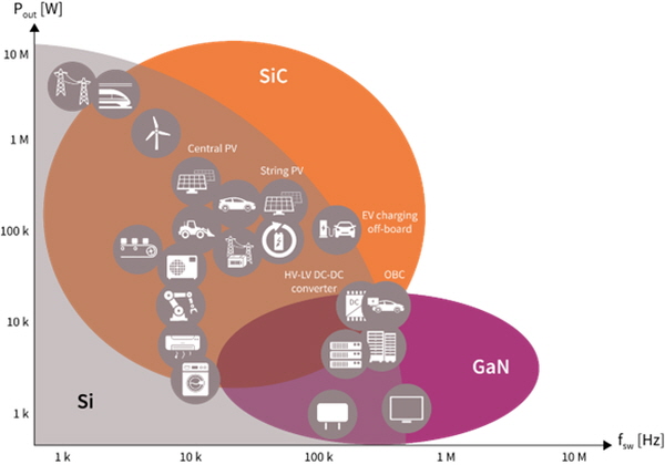
▲그림 1 : Si, SiC, GaN 각각의 적합한 애플리케이션
■ 비용과 효율
WBG 디바이스는 구입할 때 가격은 실리콘 디바이스보다 비싸지만, 더 높은 효율을 달성함으로써 전력 소모를 줄이고 냉각 필요성을 최소화하므로 수명 전반에 걸쳐서 비용을 절감하도록 한다. 전원장치 크기를 줄임으로써 운송비용을 줄인다는 점 또한 부가적인 이점이다.
그러므로 목표로 하는 애플리케이션에 WBG 디바이스를 사용함으로써 총 유지비용(TCO)을 절감하는 것이 처음에 구입할 때 실리콘 디바이스보다 가격이 더 비싼 점을 충분히 상쇄할 수 있을지 잘 따져보아야 한다. 이 계산은 각각의 활용 사례마다 달라질 것이다. 필요로 하는 전압, 전원장치로 이용할 수 있는 공간, 냉각 요구 같은 것들이 다 다를 것이기 때문이다.
예를 들어서 데이터 센터에서 전원장치 효율을 높임으로써 전기 사용을 줄이고 냉각 요구를 낮출 수 있다. 이 비용이 전체적인 가동비용에서 큰 비중을 차지한다. 실제 한 고객은 실리콘에서 WBG로 전환함으로써 전원장치 효율을 97퍼센트에서 97.8퍼센트로 높이게 되었다. 이것은 다시 말해서 초기에 더 비싼 구매 가격을 상쇄하기 위해서 약 3년의 기간이 걸린다는 뜻인데, 이 전원장치는 수명이 6∼7년에 달한다. 그러므로 WBG로 전환하는 것이 확실히 더 이득이라는 것을 알 수 있다.
■ 와이드 밴드갭을 적용한 실제 사례
○ 극히 콤팩트한 240W 충전기
그림 2에서는 실제 애플리케이션 사례로서 휴대 컨슈머 디바이스용으로 2개 USB 포트를 제공하는 극히 콤팩트한 충전기를 보여준다.
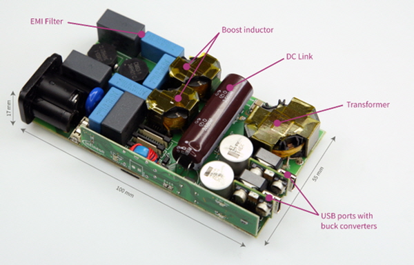
▲그림 2 : 극히 콤팩트한 충전기
최근에 EU에서는 환경과 관련한 규제가 강화됨으로써 전자 폐기물을 줄이기 위해서 컨슈머 디바이스에 범용 USB-C 충전기를 사용해야 하게 되었다. 이 충전기는 여러 디바이스를 동시에 충전할 수 있도록 충분히 높은 전력을 제공해야 한다. 5V부터 USB-PD 규격에서 정의하고 있는 최대 전압인 48V에 이르는 출력 전압을 제공해야 한다. 뿐만 아니라 90VRMS부터 265VRMS에 이르기까지 세계의 각기 다른 AC 메인 전원을 사용해서 동작할 수 있어야 한다.
USB-C 케이블은 정격이 5A이다. 그러므로 최대 48V 출력 전압으로 범용 충전기가 최대 240W를 제공할 수 있어야 한다. 이것은 오늘날 USB 충전기로 제공할 수 있는 65W 출력 전력보다 훨씬 높은 것이다.
그러기 위해서는 컨버터 디자인의 열 관리가 중요하다. 열을 발산하기 위해서 수동 대류 복사와 대류만을 사용할 수 있기 때문이다. WBG 디바이스는 더 높은 전력 밀도를 가능하게 하고 그러므로 컨버터 크기를 줄일 수 있으므로, 표면 온도가 통상적으로 70 C로 지정된 최대 온도를 넘지 않도록 해야 한다.
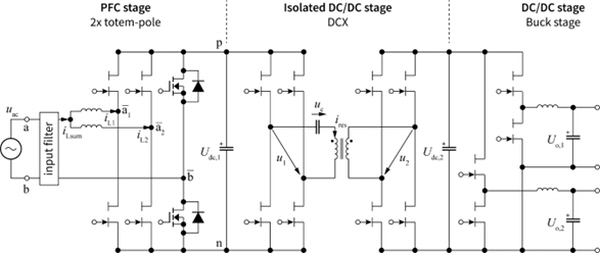
이러한 요구를 충족하기 위해서는 넓은 입력 및 출력 전압 범위를 취급하기 위해서 컨버터 디자인으로 3스테이지 접근법이 필요하다. 수동 부품의 크기를 최소화하고 그럼으로써 콤팩트한 디자인을 달성하기 위해서는 매우 높은 스위칭 주파수를 사용해야 한다.
그림 3의 충전기 디자인을 보면, PFC 스테이지는 2개 인터리브 토템폴 스테이지로 이루어지고, DCX 스테이지(DC 트랜스포머)는 연속적으로 공진 주파수로 동작하고, DC/DC 스테이지는 2개 벅 스테이지로 이루어졌다.
▲그림 3 : 극히 콤팩트한 충전기 디자인
이 디자인은 인피니언의 CoolGaN™ GIT(gate injection transistor) 기술을 채택한 CoolGaN™ IPS(integrated power stage)를 사용한다. CoolGaN GIT는 하이브리드 드레인 HEMT에다 p-GaN 게이트를 적용하고 있다. 하프 브리지 구성으로는 GIT HEMT를 사용하고, 모든 HV 소켓으로는 매칭되는 드라이버들을 사용하고, 벅 스테이지로는 CoolGaN™ 쇼트키 게이트(SG) HEMT 100V 를 사용한다.
전체 시스템이 2개 USB-C 출력 각각으로 요구되는 240W를 제공할 수 있으며 42W/inch3의 뛰어난 전력 밀도를 달성한다. 이것은 오늘날 통상적인 휴대전화 충전기로 달성할 수 있는 16W/inch3∼20W/inch3보다 훨씬 높은 것이다.
■ 데이터 센터 전원장치
또 다른 중요한 애플리케이션은 앞서도 언급했듯이 데이터 센터 전원장치이다. 클라우드 서비스, 인공 지능(AI), 암호화폐 같은 것들로 인해서 전세계적으로 데이터 센터의 처리 용량에 대한 수요가 빠르게 증가하고 있다. 이에 데이터 센터들이 서버의 전력 소모를 줄여서 비용을 절감하기 위해 고효율 전원장치에 투자하고 있다.
통상적으로 서버용으로 고효율 전원장치는 토템폴 스테이지 같은 브리지리스 PFC 스테이지와 LLC 컨버터 같은 공진 DC-DC 스테이지로 이루어진다. 12V 출력 시스템으로는 센터 탭 트랜스포머를 흔히 사용하고, 48V 출력으로는 풀브리지 정류가 훌륭한 선택이다.
그림 4에서는 54V 출력으로 7kW를 제공하는 각기 다른 서버 전원장치의 효율과 전력 밀도를 보여준다. 전부 GaN을 사용한 디자인이 효율과 전력 밀도 둘 다에 있어서 가장 우수하다는 것을 알 수 있다.
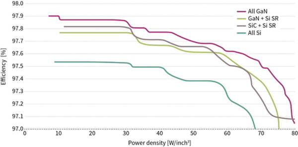
▲그림 4 : 고전력 서버 전원장치의 파레토 최적화 결과로서 전력 밀도에 따른 효율을 보여준다.
○ 극히 콤팩트한 고전력 DC-DC 서버 전원장치
그림 5는 데이터 센터용으로 또 다른 전원장치 모듈을 보여준다. 하나의 보드 크기가 89.5mm x 66.0mm x 13.5mm로서, 1.5kW를 제공하고 300W/inch3 이상의 전력 밀도를 달성한다. 10퍼센트 부하일 때 효율은 92.3퍼센트이고, 50퍼센트 부하일 때 효율은 96.7퍼센트에 달한다.
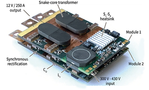
▲그림 5 : 데이터 센터용으로 극히 콤팩트한 DC-DC 전원장치 모듈
실제로 그림 5에서 보는 것은 2개 모듈을 IPOP(input-parallel output-parallel) 구성으로 결합하고 하나의 트랜스포머 코어를 공유하도록 한 것이다. 이 구성으로 이들 모듈이 12V에 250A 출력 전류로 3kW 출력 전력을 제공하고 345W/inch3의 전력 밀도를 달성한다.
이 모듈에 사용된 스네이크 코어 트랜스포머는 위상들과 모듈들 사이에 이상적인 전류 공유를 가능하게 하고, 단일 플럭스 경로에다 2개 모듈이 트랜스포머 코어를 공유함으로써 코어 손실을 낮춘다.
■ 총 유지비용 측면 WBG 이점 잘 따져야
오늘날의 전원장치 애플리케이션은 넓은 입력 및 출력 전압 범위로 극히 높은 효율과 전력 밀도를 요구한다.
GaN이나 SiC 같은 WBG 반도체는 처음에 구매할 때 가격은 실리콘 디바이스보다 높으나, 전력 소모를 낮추고 크기가 콤팩트하다는 점에서 수명 전반에 걸쳐서 총 시스템 비용을 절감하도록 한다.
그러므로 이 글에서 살펴보았듯이 기술적인 면에서뿐만 아니라 총 유지비용 측면에서도 WBG 디바이스의 이점을 잘 따져보아야 한다.
인피니언의 WBG 기술 페이지에서는 첨단 고전력 애플리케이션의 효율과 전력 밀도를 충족하도록 설계된 인피니언의 전체 와이드 밴드갭 제품 및 솔루션 포트폴리오에 관해서 더 자세한 정보를 볼 수 있다.
※ 저자
Dr. Gerald Deboy, Distinguished Engineer, 인피니언 테크놀로지스
관련뉴스
-
.jpg)
[기술기고]인피니언 테크놀로지스-와이드 밴드갭 디바이스의 특성과 동작에 대한 이해를 바탕으로 신뢰성 검증
와이드 밴드갭 디바이스의 신뢰성 검증을 위한 전문적 기술에 대해 인피니언 테크놀로지스의 Peter Friedrichs, Vice President SiC와 Tim McDonald, Senior Director(Consulting Advisor to the CoolGaN™ program)에게 들어보자.
2022-11-25 오후 12:05:05by 편집부
-

[기술기고]Eric Persson, 인피니언-GaN 기술이 가져오는 전력 변환 애플리케이션의 혁신
인피니언이 공급하는 와이드 밴드갭 갈륨 나이트라이드(GaN) 반도체인 CoolGaN™에 대해 Eric Persson Senior Principal Engineer가 소개한다.
2023-01-02 오전 9:21:24by 편집부
-
.jpg)
[기술기고]인피니언 테크놀로지스-진정한 게임 체인저로서 혁신을 예고하는 SiC 기술
인피니언 테크놀로지스가 공급하는 CoolSiC™ 기술과 CoolSiC™ 제품에 대해 인피니언의 엔지니어들이 자세히 소개한다.
2023-01-09 오후 3:09:08by 편집부


많이 본 뉴스
[열린보도원칙] 당 매체는 독자와 취재원 등 뉴스이용자의 권리 보장을 위해 반론이나 정정보도, 추후보도를 요청할 수 있는 창구를 열어두고 있음을 알려드립니다.
고충처리인 장은성 070-4699-5321 , news@e4ds.com