이종 집적에 대한 첨단 패키징 관심과 수요가 증가하고 있는 가운데 글로벌 반도체 설계 자동화 기업 케이던스와 한국 파운드리를 대표하는 삼성전자가 협업해 3D-IC 설계 개발 가속화에 나섰다.
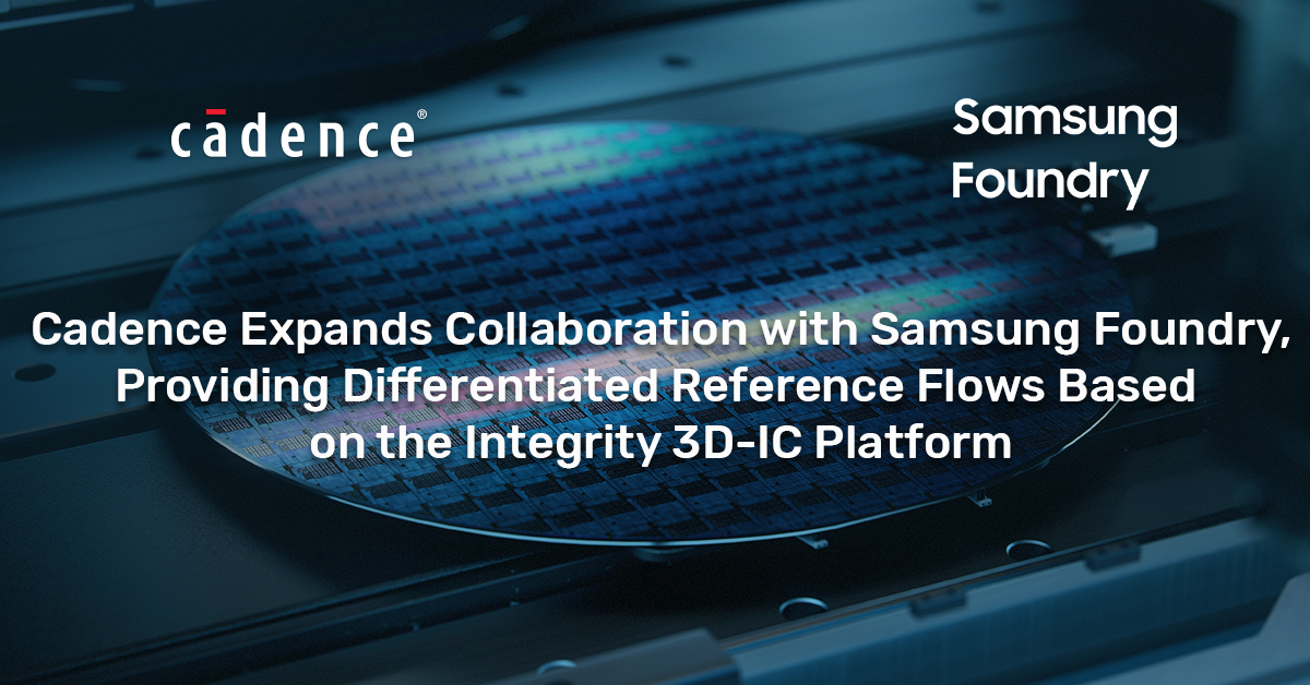
▲케이던스, 삼성 파운드리와 협업(이미지:케이던스)
케이던스 ‘인테그리티 3D-IC’ 플랫폼 제공
멀티-다이 칩 구현·첨단 패키징 개발 지원
이종 집적에 대한 첨단 패키징 관심과 수요가 증가하고 있는 가운데 글로벌 반도체 설계 자동화 기업 케이던스와 한국 파운드리를 대표하는 삼성전자가 협업해 3D-IC 설계 개발 가속화에 나섰다.
케이던스 디자인 시스템즈(Cadence Design Systems, Inc.)가 삼성 파운드리와의 협업을 확대해 △하이퍼스케일 컴퓨팅 △5G △인공지능(AI) △사물인터넷(IoT) △모바일 등의 차세대 애플리케이션을 위한 3D-IC 설계 개발을 가속화한다고 4일 발표했다.
이번 협업은 최신 레퍼런스 플로우와 관련 패키지 설계키트를 제공해 멀티-다이 (Multi-Die) 칩 개발을 촉진할 것으로 기대된다. 이는 업계 유일의 통합 플랫폼인 케이던스 ‘인테그리티 3D-IC (Cadence Integrity 3D-IC)’ 를 기반으로 하며, 시스템 계획, 패키징 및 시스템 레벨 분석을 단일 콕핏에서 제공한다.
케이던스 ‘인테그리티 3D-IC (Cadence Integrity 3D-IC)’ 플랫폼은 삼성의 새로운 3D CODE 표준을 지원한다. 이 표준은 통합된 환경에서 설계 생성 및 분석 플로우의 정의와 상호 운용성을 단순화하는 새로운 시스템 설명 언어이다.
첨단 패키지 멀티-다이 칩을 설계할 때, 엔지니어는 △설계분석 및 플로우의 복잡성 △구성 관련 과제 △시스템 수준의 열 및 전력 무결성 문제 등에 직면할 수 있다. 이 문제는 모두 설계에 소요되는 시간이 길어지는 요인이다. 이런 과제를 해결하기 위해 통합형 종합 솔루션인 △레퍼런스 플로우 △패키지 설계 키트 △삼성의 3D CODE 표준으로 멀티-다이 칩 설계와 구현 과정을 단순화해 생산성을 높이고 설계 반복 시간을 단축시킬 수 있다.
‘인테그리티 3D-IC (Cadence Integrity 3D-IC)’ 플랫폼을 기반으로 한 레퍼런스 플로우는 PDN(Power Delivery Network), LVS(Layout Versus Schematic) 및 DRC(Design Rule Checking)를 위한 초기 분석과 같은 주요 기능을 제공한다. 이러한 플로우는 ‘Cadence Allegro X 패키징 기술과 다중물리 시스템-레벨 분석 툴인 Celsius Thermal Solver 및 Clarity 3D Solver 를 통합해 추가적인 생산성 이점도 제공한다.
김상윤 삼성전자 파운드리사업부 상무는 “고성능 설계를 하는 고객들에게 저전력, 저렴한 수율 비용 및 시스템 성능 향상과 같은 고급 패키징 기술이 주는 이점을 제공하고자 한다” 며, “당사 3D CODE 기술과 케이던스의 종합적인 새로운 플로우의 도입을 통해 양사 고객들에게 멀티-다이 칩 구현 목표를 달성하고 필요한 차세대 칩 아키텍처를 제공해 빠르게 고품질 제품을 시장에 출시할 수 있도록 지원하고 있다”고 말했다.
비벡 미슈라(Vivek Mishra) 케이던스 디지털 및 사인오프 그룹의 부사장은 “케이던스는 삼성 파운드리와의 지속적인 협업을 통해 고객이 당사의 멀티-다이 칩 설계 플랫폼으로 경쟁 우위를 점하도록 지원하고 있다”며 “케이던스의 ‘인테그리티 3D-IC (Cadence Integrity 3D-IC)’ 플랫폼을 기반으로 한 레퍼런스 플로우와 삼성의 최신 기술을 결합해 고객들은 복잡한 3D-IC 설계를 생성할 때 워크플로우를 간소화하고 멀티-다이 칩 구현에 소요되는 시간을 단축하는 통합된 설계 환경을 이용할 수 있다”고 말했다.