기사입력 2023.09.04 10:33
.JPG)
[편집자주] EMC(Electromagnetic Compatibility, 전자파 적합성)를 비롯한 SI/PI 등의 관련 전문가들로 구성된 한국전자파학회 EMC기술연구회서는 매년 EMC 기술을 교류하고 기술 확산에 기여하고 있다. 최근 자동차의 전장화 추세와 더불어 소형화 및 고집적·고전력 제품의 증가로 EMI·EMC 측면에서 해결해야 할 문제들이 점차 증가하고 있는 가운데 EMC기술연구회의 연례행사인 EMC KOREA 2023가 개최를 앞두고 있다.
2023-07-04 오후 4:59:03by 권신혁 기자
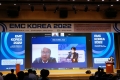
제품의 소형화와 대전력화 추세가 계속되며 EMI·EMC 측면에서 해결해야 할 문제들은 점차 증가하고 있다. 국내 EMC 전문가들이 총집합하는 EMC KOREA 2023이 개최를 앞두며, 최신 EMC 기술과 해결책에 대한 관심이 고조되고 있다.
2023-07-05 오후 4:55:15by 권신혁 기자
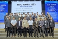
국내 EMC기술 행사 가운데 전통과 역사를 자랑하는 한국전자파학회의 EMC KOREA 2023이 개최돼 전국의 수많은 EMC 기술자와 연구자들이 한데 모였다.
2023-07-14 오전 9:13:45by 권신혁 기자

[열린보도원칙] 당 매체는 독자와 취재원 등 뉴스이용자의 권리 보장을 위해 반론이나 정정보도, 추후보도를 요청할 수 있는 창구를 열어두고 있음을 알려드립니다.
고충처리인 장은성 070-4699-5321 , news@e4ds.com