세계 최대 규모의 반도체 메가 클러스터 구축 청사진이 점차 구체화되고 있다. 최근 세부 조성 방안이 발표되며 국내 반도체 산업이 글로벌 허브로 도약하는 기점이 될지 이목이 집중되고 있다.
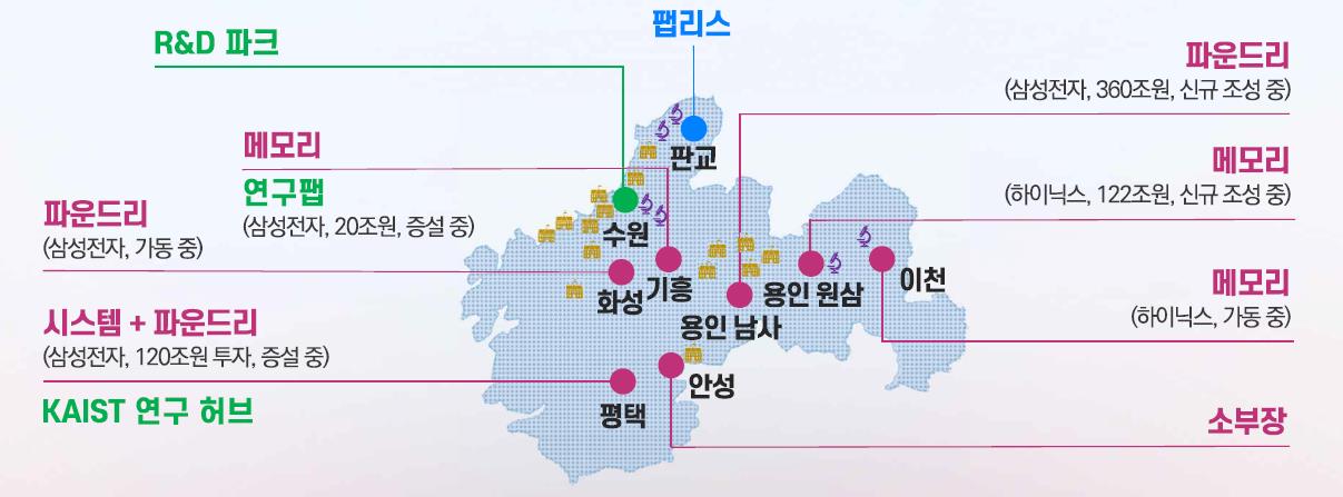
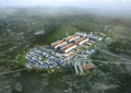
▲경기 남부 반도체 메가 클러스터 지도(이미지:산업부)
2030년 月 770만장 웨이퍼 생산 목표
파운드리-팹리스-소부장 공급망 강화
미래 AI·화합물 반도체 기술 확보 전략
세계 최대 규모의 반도체 메가 클러스터 구축 청사진이 점차 구체화되고 있다. 최근 세부 조성 방안이 발표되며 국내 반도체 산업이 글로벌 허브로 도약하는 기점이 될지 이목이 집중되고 있다.
지난 15일 반도체 인재양성 현장에서 정부가 ‘반도체 메가 클러스터 조성방안’을 발표했다.
반도체 메가 클러스터는 경기 남부 지역인 △평택 △화성 △용인 △이천 △안성 △성남 판교 △수원 등 반도체 기업과 관련 기관이 밀집한 지역 일대를 일컫는다. 현재 19개의 생산팹과 2개의 연구팹이 집적된 메가 클러스터에는 2047년까지 총 622조원의 민간 투자를 통해 생산팹 13개와 연구팹 3개가 신설될 예정이다. 2027년에는 생산팹 3기, 연구팹 2기가 완공될 전망이다.
■ 생산유발 효과 650조원·직간접 고용 346만명 기대
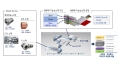
▲반도체 메가 클러스터 전력공급계획(이미지:산업부)
메가 클러스터는 2,102만 제곱미터 면적으로 2030년까지 월 770만장의 웨이퍼 생산을 목표로 하고 있는 것으로 알려졌다. 정부는 650조원의 생산 유발효과를 전망하며 소부장·협력기업 매출 204조원 확대와 팹 운영 직접 인력 11만명에 346만명의 직·간접적인 고용 창출을 기대했다.
이는 팹에 들어가는 장비 생산과 원자재 제조업체의 생산 증대에 따른 약 193만명의 직접 고용 창출과 주변 지역 상권이 활성화됨과 동시에 도로·전력·공업용 등 인프라 건설 확대에 약 142만명의 간접 고용 창출 효과가 발생할 것으로 추정한 수치이다.
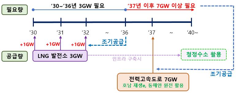
현재 신규 조성을 추진하는 용인 국가산단과 일반산단에는 총 10GW 이상의 전력과 하루 110.8만톤의 용수가 추가로 필요해 이에 대한 공급 계획을 지난 12월 확정했다.
정부는 반도체 등 첨단산업 시설투자 세액공제율을 최대 25%로 높이고 현재 22개인 반도체 세액공제 대상 기술(국가전략기술)을 확대할 계획이라고 밝혔다. 아울러 도로·용수·전력 등 기반시설에 대한 국비 지원을 강화하며, 올해 반도체 예산을 2022년 대비 2배 규모로 확대한 1.3조원을 편성한 것으로 진해진다.
■ 파운드리-팹리스-소부장 공급망 강화 도모
현재 30% 수준인 공급망 자립률은 반도체 공급망 리스크 노출로 이어지고 있다. 이에 2030년까지 공급망 자립률 50%까지 끌어올리는 한편, 현재 4개 기업인 1조 매출 클럽을 10개 기업까지 늘리는 것을 목표로 정부에서 메가 클러스터를 활용한 소부장 기업 육성 전략을 추진할 전망이다.
공백상태에 있는 양산 검증 지원을 위한 테스트베드를 2027년 완공을 목표로 추진할 계획인 것으로 보이며, 예비타당성 조사를 거쳐 총 사업비 9천억원 규모로 용인 클러스터 내에 구축될 예정이다.
외국인 투자유치 확대를 위해 2,000억원 규모의 인센티브를 조성해 글로벌 장비기업 R&D 센터 유치를 통해 국내 부족한 기술력을 보완할 수 있을 것으로 기대했다.
또한 파운드리-팹리스 간 밸류체인을 완성해 시스템반도체 시장 점유율을 2030년까지 10%로 확대하고 글로벌 매출액 상위 50위 안에 들어가는 팹리스 기업을 10개사까지 육성하는 것을 목표로 삼았다.
이를 위해 팹리스가 개발한 칩 성능 검증을 위한 ‘검증지원센터’를 신규로 구축할 계획이다. 또한 팹리스 시제품 제작비 국비 지원 규모 2배 확대, 첨단칩 개발 지원을 위한 초미세 공정 국비 지원 트랙 신설, 파운드리 기업들의 시제품 제작 개방 횟수 확충을 병행해 팹리스 지원체계를 구축할 것으로 보인다.
자금지원과 관련해서는 대출·보증을 우대 지원하는 정책금융을 3년간 총 24조원으로 확대하고, 최대 1.3%p의 우대금리를 제공할 예정이다.
■ 차세대 반도체 초격차 기술 확보 전략
정부는 세계 최고 수준의 저전력, 고성능의 국산 AI반도체를 개발 및 실증하는 ‘K-클라우드 프로젝트’를 추진할 것이라고 밝혔다.
과기부는 국산 AI 반도체를 2030년까지 단계적으로 고도화(NPU→PIM→극저전력 PIM) 하는 것을 목표로 삼았다. 이를 데이터 센터에 적용해 AI 반도체의 기술과 성능을 검증할 예정으로 검증된 기술은 △지능형 교통관제 △지능형 CCTV △AI 디지털 교과서 등 국민 생활과 밀접한 분야에 우선 적용할 계획이다.
고도화된 국산 AI 반도체에 특화된 클라우드 데이터센터 HW·SW 핵심기술을 확보해 높은 수준의 기술생태계 완성을 목표했다. 약 1조원 규모의 ‘K-클라우드’ 기술개발 예타도 추진 중이다.
과기부는 글로벌 최고 수준의 GPU 대비 △AI 서비스 전력 소모 1/10로 감소 △AI 학습 효율 2배 향상을 달성하겠다는 계획이다.
더불어 성균관대, 경희대, 아주대 등과 함께 화합물반도체 특화 연구 인프라인 한국나노기술원 등이 소재해 있는 수원을 화합물 반도체 기술 거점으로 발전시킬 계획이다. 메가클러스터를 중심으로 대전, 광주, 부산, 포항 등 지역별 집적단지와 유기적인 협업 체계를 구축하고, R&D-실증-분석 전주기를 지원해 우주·국방, 통신, 전력, 센서 등 4대 전략분야 중심으로 성과를 창출할 것이라고 밝혔다.
이외에도 KAIST 평택 캠퍼스를 2029년까지 설립하고 카이스트 차세대 설계 연구센터 및 소자 연구센터를 구축한다. 아울러 전국적으로 산재해 있는 국가 반도체 연구 인프라를 온라인으로 연계·통합(MoaFab 서비스)하고, 민간 팹과의 협업을 통해 인프라 서비스를 지속적으로 개선할 계획이다.