최근 첨단 반도체 파운드리 공정에서 1~2나노 차세대 기술 로드맵을 발표하며 초미세 패터닝에서 옹스트롬 시대가 열렸다. 인텔이 1.8나노에 해당하는 18옹스트롬 기반 로드맵을 본격화하는 가운데 이를 뒷받침하는 소재·장비사 기술 혁신 또한 발빠르게 기술 한계를 뛰어넘고 있다.
▲박광선 어플라이드 머티어리얼즈 코리아 대표
브릿지 결함 제거로 패터닝 비용↓
EUV 라인 에지 러프니스 해결 必
패터닝 유효시장 규모 80억달러↑
최근 첨단 반도체 파운드리 공정에서 1~2나노 차세대 기술 로드맵을 발표하며 초미세 패터닝에서 옹스트롬 시대가 열렸다. 인텔이 1.8나노에 해당하는 18옹스트롬 기반 로드맵을 본격화하는 가운데 이를 뒷받침하는 소재·장비사 기술 혁신 또한 발빠르게 기술 한계를 뛰어넘고 있다.
어플라이드 머티어리얼즈가 4일 경기도 성남시 분당에 위치한 한국지사 사무실에서 미디어 브리핑을 개최했다.
이날 브리핑에서는 옹스트롬 시대 칩 제조를 위한 어플라이드 머티어리얼즈의 패터닝 솔루션 포트폴리오 확대를 밝히고 스컬프타(Sculpta)·심3 와이 매그넘(Sym3 Y Magnum)·아셀타(Aselta)·프로듀서 XP 파이오니어 CVD(Producer XP Pioneer CVD) 등을 소개했다.
기존에 없던 새로운 식각 시스템을 통해 EUV 및 하이 NA EUV 리소그래피 관련 공정 효율을 향상시키고 결함(Defect)을 줄이는 솔루션을 통해 어플라이드 머티어리얼즈는 올해 2억달러 매출을 예상했으며, 2025년 매출은 5억달러를 전망했다.
박광선 어플라이드 머티어리얼즈 코리아 대표는 “초미세 패터닝을 구현하는 EUV를 더 잘 구현하기 위해서는 몇몇 기술들이 필요하다”면서 “어플라이드의 기술은 패터닝과 관련해 10여년전부터 생태계 협업을 통해 준비한 기술들이 많으며 그러한 협업의 결과 이러한 새로운 식각 기술을 통해 고객사의 로드맵과 비용절감을 제공하게 될 것이다”라고 말했다.
■ 스컬프타, 브릿지 결함 제거로 패터닝 비용↓
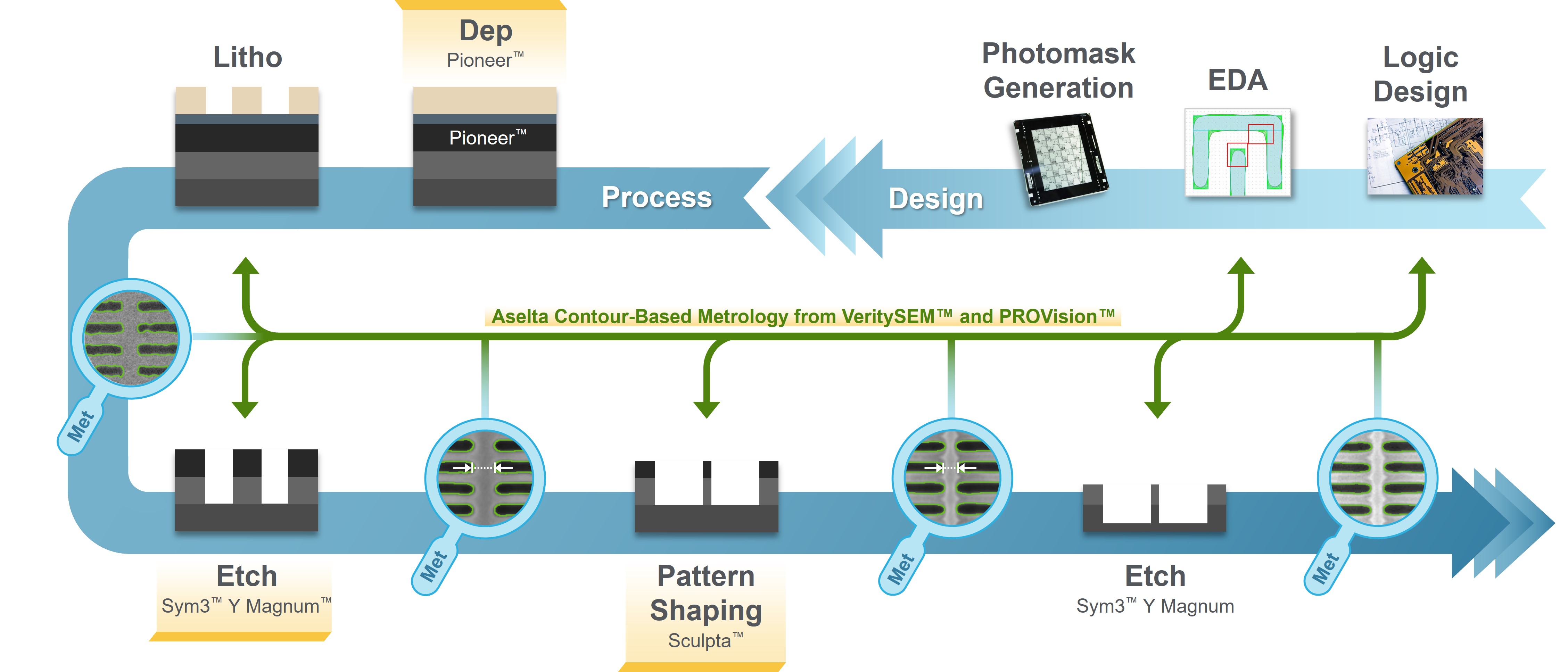
▲패터닝 공정 흐름(자료:어플라이드)
지난해 어플라이드는 EUV 더블 패터닝 단계를 줄여 싱글 EUV 또는 하이 NA EUV 노광 대비 팁 간격을 좁힐 수 있는 ‘센튜라 스컬프타(Centura Sculpta)’ 패터닝 시스템을 발표한 바 있다.
현재 스컬프타 장비는 전세계 리딩 엣지 고객사에 적용된 것으로 전해지며 관련 애플리케이션을 확장 중에 있다고 설명했다. 스컬프타 채택의 이점은 팁 간격을 줄이는 것뿐 아니라 반도체 제조사들이 브릿지 결함을 제거해 패터닝 비용을 절감하고 칩 수율을 개선할 수 있다는 것에 있다.
인텔은 옹스트롬 공정 위해 스컬프타 시스템을 도입했다고 밝혔으며, 처리량·웨이퍼 수율·비용 등의 면에서 개선효과가 있었다고 언급했다. 삼성전자는 4나노 공정에 스컬프타 시스템을 도입해 평가하고 있는 것으로 알려져 있다.
이길용 어플라이드 머티어리얼즈 기술마케팅 및 전략 프로그램 총괄은 “웨이퍼에 패턴을 잘 전사하는 것 자체가 어려우며 EUV 리소그래피가 직면한 문제는 ‘확률적(Stochastic)’으로 발생하는 결함이 챌린지”라며 “이러한 임의변이는 라인 에지 러프니스와 금속 라인 사이에 브릿지를 형성해 다양한 결함으로 이어진다”고 설명했다.
■ EUV 라인 에지 러프니스 해결 必
▲이길용 어플라이드 머티어리얼즈 기술마케팅 및 전략 프로그램 총괄(사진:어플라이드)
라인 에지 러프니스가 크면 전자 저항이 높아지며 거친 라인 에지가 웨이퍼에 식각되면 단선, 단락 회로가 형성될 수 있다. 이와 같은 결함 형태의 경우 최근 제조사들이 라인과 패턴 간격을 더욱 좁히면서 발생 빈도가 더욱 높아지고 있는 상황이다.
어플라이드는 동일 챔버에서 증착과 식각을 모두 지원하는 심3 와이 매그넘 식각 시스템을 출시해 거친 에지에 물질을 증착해 EUV 라인 패턴을 매끄럽게 만들어 수율을 높이고 라인 저항을 감소시키는 효과를 주고 있다.
현재 심3 와이 매그넘은 주요 반도체 제조사들이 파운드리 로직에서 채택하고 있으며 D램 EUV 패터닝에선 가장 널리 채택된 식각 기술이기도 하다.
여기에 더해 프로듀서 XP 파이오니어 CVD 패터닝 필름을 조합할 때 패턴 균일성을 최적화할 수 있는 것으로 전해졌다. 파이오니어 필름은 첨단 공정에서 사용되는 식각 화학 물질에 대해 탄성력이 높은 고밀도 카본을 기반으로 측벽 패턴 형태 균일도가 뛰어나면서도 기존 보다 얇은 두께의 스펙을 가지고 있다.
주요 메모리 제조사들이 파이오니어를 채택해 D램 패터닝에 이용하고 있다. 파이오니어는 스컬프타 및 심3 와이 매그넘과 조합돼 패터닝 최적화에 선택지를 높여주고 있는 것으로 전해졌다.
■ 옹스트롬 시대 계측, 미세 정렬 지원
초미세 공정에서의 또다른 과제는 각 층마다 수십억 개의 형상을 빈틈없이 정의하고 배치하는 것이다. 여러 층으로 이뤄진 패터닝 공정에서 다음 층과 정확하게 정렬하는 것이 중요하며 작은 배치 오류는 칩의 성능에 큰 영향을 미치며 더 나아가 수율에도 악영향을 미치는 결함까지도 발생할 수 있다.
어플라이드는 전자빔 계측 시스템을 통해 로직 및 메모리 EUV 패터닝에서 솔루션 한 축을 담당하고 있다. 설계 기반 계측 기술 기업 아셀타 나노그래픽스(Aselta Nanographics)를 인수했다고 밝히며 컨투어를 통한 패터닝 필름과 웨이퍼에서 각각의 레시피가 만들어내는 형상에 대해 몇 배 더 많은 데이터를 수집할 수 있다고 강조했다.
아셀타 컨투어 기술은 현재 어플라이드 베리티 SEM 등 전자빔 계측 시스템에 통합돼 반도체 제조사에 초미세 공정을 포함한 광범위한 계측 문제 해결에 엔드 투 엔드 기능을 제공한다고 설명했다.
한편, 어플라이드에 따르면 패터닝 유효시장 규모는 CVD, ALD, 식각 및 선택적 제거 등 4종 재료 제거, 열 공정, 전자빔 계측 등을 포함해 10년 전 15억달러 규모에서 현재는 80억달러 이상의 규모로 성장한 것으로 나타났다.