기사입력 2024.05.20 09:00
첨단 반도체 전문기업 네패스(회장 이병구)가 서울특별시교육청(교육감 조희연)과 반도체 전문기술인력 양성 및 직업교육 체제 구축을 위해 손을 맞잡았다.
2023-04-25 오전 11:42:23by 배종인 기자
인텔, 네패스, 어플라이드 머티어리얼즈, 현대차증권, 차세대지능형반도체사업단, 한양대학교가 참여하는 반도체 패키징 전문 세미나인 ‘2023 e4ds 반도체 패키징 데이’가 오는 6월28일 수요일 한국컨퍼런스센터 대강당에서 개최된다.
2023-06-07 오전 9:43:12by 편집부
.jpg)
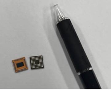
반도체 후공정 기업 네패스가 최근 미국 글로벌 팹리스로부터 인공지능(AI) 칩셋용 전력 반도체 수주를 시작으로 고성능 컴퓨팅(HPC), 자동차 등 첨단 패키징 시장 확대에 본격적으로 나선다.
2024-02-26 오후 2:11:23by 배종인 기자
네패스가 전량 수입에 의존하고 있는 기능성 반도체 재료인 도금액을 오랫동안 자체 연구개발과 협업으로 국산화해 2년 전부터 초도 생산을 해오다 HBM용 TSV 공장에 채택됨으로 올해부터 본격 양산을 시작한다.
2024-04-04 오전 8:14:38by 배종인 기자

네패스가 인공지능(AI) 반도체용 PMIC를 대량 수주하며, 600억원 이상의 투자에 본격 나선다.
2024-04-15 오전 9:49:42by 배종인 기자

[열린보도원칙] 당 매체는 독자와 취재원 등 뉴스이용자의 권리 보장을 위해 반론이나 정정보도, 추후보도를 요청할 수 있는 창구를 열어두고 있음을 알려드립니다.
고충처리인 장은성 070-4699-5321 , news@e4ds.com


