기사입력 2024.05.24 15:06
MBD는 차량 기능을 여러 블록으로 분리하고 각 블록을 연결해 전체 차량 작동을 확인한다. 전장품의 성능을 평가하려면 개별 블록의 반도체 작동을 포함하는 세부적인 시뮬레이션 모델이 필요하다. 그러나 모델이 더욱 상세해지고 정밀해지며 검증 시간이 길어지고 있다. 이에 도시바가 검증 시간을 약 90% 단축하는 애큐-롬 기술을 개발했다.
2021-09-24 오전 10:50:09by 이수민 기자
.jpg)
2025년 300㎜ 반도체 웨이퍼 생산량이 정부 지원 및 인센티브 프로그램 등으로 인한 강력한 성장세로 신기록을 달성할 것으로 전망된다.
2022-10-13 오후 2:09:36by 배종인 기자

지능형 전력 및 센싱 기술의 선도 기업인 온세미가 글로벌파운드리(GlobalFoundries, GF)의 미국 뉴욕 제조 시설을 인수하며, 온세미의 전력, 아날로그 및 센싱 기술의 성장 가속화 및 차별화에 나섰다.
2023-02-15 오후 4:25:26by 배종인 기자
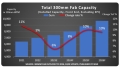
SEMI가 발표한 300㎜ 팹 전망 보고서에 따르면 2026년에 300㎜팹의 생산능력이 월 960만장으로 역대 최대치를 기록할 것으로 나타났다.
2023-03-29 오후 4:23:29by 배종인 기자

텍사스 인스트루먼트(TI)의 새로운 300㎜ 반도체 웨이퍼 제조 공장인 RFAB2가 LEED(Leadership in Energy and Environmental Design) 건축물 인증제도 버전 4(v4)에 따라 상위 등급인 골드(Gold) 등급 인증을 획득하며 그간 친환경 및 지속가능한 제조를 위한 오랜 노력의 결실을 거뒀다.
2023-09-04 오후 12:32:36by 배종인 기자

텍사스 인스트루먼트(TI)는 미국 유타주 리하이에서 새로운 300mm 반도체 웨이퍼 제조 공장(팹) 착공식을 개최했다고 6일 밝혔다.
2023-11-06 오전 9:44:21by 권신혁 기자
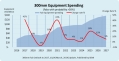
글로벌 전자 산업 공급망을 대표하는 산업 협회인 SEMI의 최신 자료에 따르면 전 세계 300㎜ 팹 장비 투자액이 2025년 처음으로 1,000억 달러를 넘어선 후 2027년에는 1,370억 달러를 기록할 것으로 예상됐다.
2024-03-25 오후 3:34:19by 배종인 기자

[열린보도원칙] 당 매체는 독자와 취재원 등 뉴스이용자의 권리 보장을 위해 반론이나 정정보도, 추후보도를 요청할 수 있는 창구를 열어두고 있음을 알려드립니다.
고충처리인 장은성 070-4699-5321 , news@e4ds.com


