기사입력 2024.09.12 16:46

인피니언은 8억3,000만달러에 GaN Systems Inc를 인수하는 계약을 체결했다고 3일 발표했다.
2023-03-03 오후 2:06:34by 성유창 기자
인피니언이 CoolGaN™ 600V HD-GIT(하이브리드-드레인-임베디드 게이트 주입 트랜지스터) 기술을 자체 제조 설비에 성공적으로 통합하며, 고품질 GaN 포트폴리오를 출시한다.
2023-06-01 오후 12:23:47by 배종인 기자

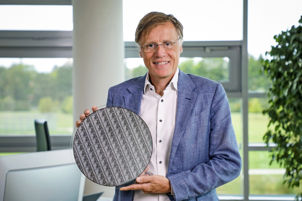
인피니언 테크놀로지스(이하 인피니언)가 선도적인 GaN 기술을 보유하고 있는 기업을 인수하며 전력 반도체 분야에서의 입지를 굳건히 다져 나간다.
2023-10-26 오전 11:06:52by 성유창 기자
향후 5년간 46%의 연평균 성장률(Yole Group 전망)로 성장이 예상되는 GaN 디바이스 시장에서 인피니언 테크놀로지스(이하 인피니언)는 CoolGaN의 강점과 생산 용량을 더욱 확장할 것이라 밝혔으며, 이 계획의 일부인 새로운 CoolGaN 제품군을 선보인다.
2024-06-04 오전 9:44:40by 성유창 기자
인피니언 테크놀로지스(코리아 대표이사 이승수)가 시중의 다른 GaN(갈륨나이트라이드, 질화갈륨) 제품 대비 입력 및 출력 FoM(figures-of-merit)이 20% 더 우수한 가성비 있는 새로운 CoolGaN™ 트랜지스터 700V G4 제품군을 새롭게 선보이며, 컨슈머 전원 장치에서 최고의 성능을 보장한다.
2024-07-01 오전 11:42:52by 배종인 기자

글로벌 반도체 기업인 인피니언 테크놀로지스(Infineon Technologies)와 중국의 이노사이언스(Innoscience)의 특허침해 소송이 단순한 기술 침해를 넘어 미래 인공지능(AI) 서버 및 데이터센터용 GaN(질화갈륨, 갈륨나이트라이드) 전력반도체 시장 선점에 중요한 분수령이 될 것으로 분석된다.
2024-08-08 오전 11:27:09by 배종인 기자
인피니언 테크놀로지스(코리아 대표이사 이승수)의 650V CoolGaN™ 트랜지스터가 비테스코 테크놀로지스의 DCDC 컨버터에 사용되며, 시스템 성능을 크게 향상시키고, 시스템 비용을 최소화했다.
2024-08-19 오전 10:10:26by 배종인 기자

[열린보도원칙] 당 매체는 독자와 취재원 등 뉴스이용자의 권리 보장을 위해 반론이나 정정보도, 추후보도를 요청할 수 있는 창구를 열어두고 있음을 알려드립니다.
고충처리인 장은성 070-4699-5321 , news@e4ds.com


