기사입력 2025.02.05 10:19


키사이트가 16일 ‘키사이트 월드 테크 데이 2024’틀 통해 통신, 오토모티브, AI 분야에서 첨단기술을 소개했다. 이날 이선우 키사이트코리아(Keysight) 대표이사 사장은 “세상을 연결하고 연결된 세상에서 세상이 안전하게 돌아갈 수 있도록 키사이트는 산업 발전을 위해 진심으로 투자하고 있다”고 밝혔다.
2024-10-16 오후 12:14:19by 배종인 기자
.jpg)
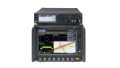
키사이트테크놀로지스가 PNA-X 벡터 네트워크 분석기 포트폴리오에 새로운 NA520xA PNA-X를 추가했다.
2024-11-12 오후 5:50:20by 배종인 기자
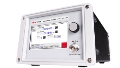
키사이트테크놀로지스가 RF 아날로그 신호 발생기와 마이크로웨이브 아날로그 신호 발생기 등 두 가지 새로운 아날로그 신호 발생기를 출시하며 포트폴리오를 확장했다.
2024-12-09 오후 3:10:00by 배종인 기자
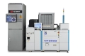
키사이트테크놀로지스가 3kV 고전력 웨이퍼 테스트가 가능한 4881HV 고전압 웨이퍼 테스트 시스템을 출시하며, 전력 반도체 생산성 및 효율성 향상이 기대된다.
2024-12-12 오전 9:25:26by 배종인 기자
.jpg)
키사이트 Advanced Design System(ADS)과 지멘스 Xpedition Enterprise EDA 도구 모음 간의 통합을 통해 엔지니어들이 Xpedition에서 레이아웃 및 제조를, 키사이트 ADS에서 RF 회로 및 전자기 시뮬레이션을 수행, 디지털 시스템과 RF 회로를 더 효율적으로 공동 설계할 수 있게돼 향후 개발자들이 5G/6G 및 레이더 시스템 등 차세대 무선 설계에서 성능 최적화를 달성할 수 있을 것으로 기대가 모아진다.
2024-12-19 오전 9:22:57by 배종인 기자

키사이트가 인공지능(AI), 고성능 컴퓨팅(HPC), 데이터센터 인터커넥트(DCI), 네트워크 인프라를 테스트하는 다중 포트, 다중 사용자, 다양한 속도를 제공하는 테스트 및 검증 플랫폼인 ‘인터커넥트 및 네트워크 성능 테스터 800GE 솔루션’을 출시했다.
2025-01-10 오전 9:56:09by 배종인 기자
키사이트테크놀로지스와 새솔테크가 자동차 인증서를 혁신적으로 관리하는 개념 증명(Proof of Concept, PoC)을 성공적으로 수행했다.
2025-01-17 오후 4:33:55by 배종인 기자

[열린보도원칙] 당 매체는 독자와 취재원 등 뉴스이용자의 권리 보장을 위해 반론이나 정정보도, 추후보도를 요청할 수 있는 창구를 열어두고 있음을 알려드립니다.
고충처리인 장은성 070-4699-5321 , news@e4ds.com


