기사입력 2025.05.09 13:12
.jpg)

인텔(Intel)이 18A 공정 기술 기반 에릭슨의 5G SoC를 생산하는 등 차세대 5G 인프라 최적화로 협력 확대에 본격 나선다.
2023-07-28 오후 12:32:17by 배종인 기자

앤시스가 시높시스와 협력해 삼성전자 파운드리 사업부와 함께 14LPU 공정 기술을 위해 개발한 무선 주파수 집적 회로(RFIC) 설계를 위한 새로운 레퍼런스 플로우(reference flow)를 출시했다.
2023-10-16 오후 12:33:07by 배종인 기자
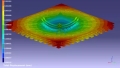
글로벌 엔지니어링 시뮬레이션 선도 기업인 앤시스코리아(대표 문석환)가 첨단 병렬(2.5D) 및 3D 집적 회로(3D-IC) 시스템의 전력 및 열 관리에 긴밀히 협력하며, 삼성전자 파운드리 제품의 성능과 신뢰성 향상에 기여한다.
2023-10-23 오전 10:32:39by 배종인 기자

앤시스코리아(대표 문석환)는 삼성전자 파운드리 사업부가 8㎚(나노미터) LN08LPP Low Power Plus 실리콘 공정으로 제조된 초고속 제품 해석을 위한 앤시스의 온칩 전자기(EM, electromagnetic) 디자인 솔루션인 ‘랩터X(RaptorX)’를 인증했다고 발표했다.
2023-12-07 오전 9:12:18by 배종인 기자

인텔 18A 공정 기반의 주력 제품인 AI PC용 프로세서인 ‘팬서 레이크(Panther Lake)’와 서버용 프로세서인 ‘클리어워터 포레스트(Clearwater Forest)’가 운영 체제를 성공적으로 부팅했다.
2024-08-07 오후 1:45:34by 배종인 기자
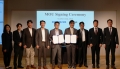
글로벌 엔지니어링 시뮬레이션 선도 기업인 앤시스코리아(대표 박주일)와 삼성SDS(대표 황성우)가 삼성SDS 클라우드 기반에 앤시스 CAE 솔루션을 공급 및 기술지원하며, 방산 및 국방 분야 클라우드 사업에서 손을 맞잡았다.
2024-10-23 오전 8:19:12by 배종인 기자
.PNG)
인텔(Intel)이 18A(옹스트롬) 기술을 적용한 팬서레이크(Panther Lake)를 2025년 하반기 예정대로 출시한다며, 기술에 있어 자신감을 보였다.
2025-03-21 오전 10:33:13by 배종인 기자

인텔이 29일 미국 산호세에서 개최된 ‘인텔 파운드리 다이렉트 커넥트(Intel Foundry Direct Connect)’ 행사에서 차세대 반도체 공정과 첨단 패키징 기술을 공개하며 글로벌 제조 및 공급망 역량을 강조했다. 인텔은 18A 및 14A 공정을 본격 추진하고, 첨단 패키징 기술로 시스템 수준 통합을 제공한다. 또한 미국 내 제조 역량 강화에 나서며 2026년 애리조나 공장을 가동한다.
2025-04-30 오후 4:55:09by 배종인 기자

[열린보도원칙] 당 매체는 독자와 취재원 등 뉴스이용자의 권리 보장을 위해 반론이나 정정보도, 추후보도를 요청할 수 있는 창구를 열어두고 있음을 알려드립니다.
고충처리인 장은성 070-4699-5321 , news@e4ds.com