기사입력 2025.04.30 16:55
.jpg)
인텔은 이사회가 립부 탄(Lip-Bu Tan)을 신임 CEO로 임명했다고 13일 밝혔다. 립부 탄 CEO는 18일부터 공식 업무를 시작하며, 인텔 이사회에도 합류한다.
2025-03-13 오후 12:19:14by 권신혁 기자
.jpg)
인텔(Intel)이 현대 기업의 복잡한 애플리케이션 아키텍처 전반에서 높은 신뢰성과 보안을 제공하는 통합 솔루션 제품군인 인텔® 타이버™ 트러스트 서비스(Intel® Tiber™ Trust Services) 포트폴리오의 확장을 발표했다.
2025-03-14 오후 3:28:42by 배종인 기자
인텔(Intel)이 새로운 인텔® AI 엣지 시스템(Intel® AI Edge Systems), 엣지 AI 스위트(Edge AI Suites) 및 오픈 엣지 플랫폼(Open Edge Platform) 이니셔티브에 대한 내용을 발표하며, AI와 기존 인프라의 통합을 한층 간소화했다.
2025-03-20 오전 11:19:17by 배종인 기자
.PNG)
인텔(Intel)이 18A(옹스트롬) 기술을 적용한 팬서레이크(Panther Lake)를 2025년 하반기 예정대로 출시한다며, 기술에 있어 자신감을 보였다.
2025-03-21 오전 10:33:13by 배종인 기자
.jpg)
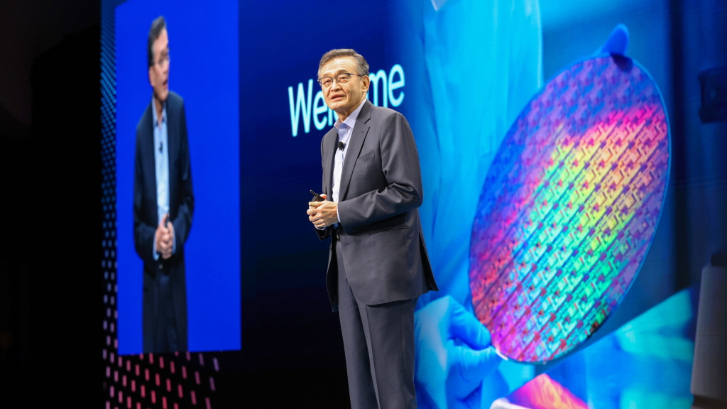
인텔 립부 탄(Lip-Bu Tan) 인텔 CEO가 미국 라스베이거스에서 현지 시간 31일 개최된 ‘인텔 비전(Intel Vision) 2025’ 오프닝 키노트에서 고객 중심과 엔지니어링 우수성에 기반한 비전을 1일 발표했다.
2025-04-01 오전 11:40:23by 권신혁 기자

AI 도입이 가속화됨에 따라, CPU는 데이터 전처리, 전송, 시스템 오케스트레이션 등 핵심 기능을 관리하는 호스트 노드로서 AI 시스템 운영에 필수적이다. 인텔은 MLPerf에 서버용 CPU 성능 결과를 제출한 유일한 반도체 업체로서 차별성을 이어가고 있다.
2025-04-07 오전 11:21:41by 권신혁 기자

인텔(Intel)이 상하이 모터쇼 2025에서 업계 최초로 멀티-공정 노드 칩렛 아키텍처를 적용한 2세대 인공지능(AI) 강화 소프트웨어 정의 차량(SDV) SoC를 공개했다. 이 신형 SoC는 지능형 커넥티드 차량에 대한 수요 증가에 발맞춰 설계됐으며, 완성차 업체에 확장가능한 성능, 첨단 AI 기능, 비용 효율성을 제공한다.
2025-04-24 오후 2:30:54by 배종인 기자

[열린보도원칙] 당 매체는 독자와 취재원 등 뉴스이용자의 권리 보장을 위해 반론이나 정정보도, 추후보도를 요청할 수 있는 창구를 열어두고 있음을 알려드립니다.
고충처리인 장은성 070-4699-5321 , news@e4ds.com


