기사입력 2025.05.09 14:03
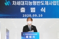
과기정통부와 산업부가 경기도 성남시에 위치한 반도체산업협회에서 차세대지능형반도체사업단 출범식을 열고 차세대 지능형 반도체 개발과 이를 뒷받침할 생태계 구축을 위한 MOU를 체결했다. 사업단이 총괄하는 차세대 지능형 반도체 기술개발 사업에는 10년간 1조96억 원이 투입된다.
2020-09-11 오후 2:14:23by 이수민 기자
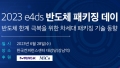
인텔, 네패스, 어플라이드 머티어리얼즈, 현대차증권, 차세대지능형반도체사업단, 한양대학교가 참여하는 반도체 패키징 전문 세미나인 ‘2023 e4ds 반도체 패키징 데이’가 오는 6월28일 수요일 한국컨퍼런스센터 대강당에서 개최된다.
2023-06-07 오전 9:43:12by 편집부
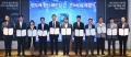
산업통상자원부, 삼성전자, SK하이닉스, LG화학, 하나마이크론, 프로텍, 사피온코리아, 심텍, 차세대지능형반도체사업단, 한국반도체산업협회, 한국산업기술평가관리원 등 소부장, 반도체 후공정 전문업체(OSAT) 및 팹리스 기업 등이 참여해 ‘반도체 첨단 패키징 기술개발 협력에 관한 협약’을 체결했다.
2023-08-29 오후 1:34:45by 배종인 기자
.jpg)
대구경북과학기술원(DGIST, 총장 이건우) 화학물리학과 유천열 교수 연구팀이 자성메모리 동작을 위한 스핀-궤도 토크를 전기장을 인가해 초고효율로 온-오프 제어하는 기술을 개발하는 데 성공했다. 이번 연구 결과는 세계적 권위 국제학술지 ‘Science Advances’에 3월19일 온라인판에 게재됐다. 이번 연구결과는 차세대지능형반도체기술개발(소자)사업의 지원을 받아 수행하여 ‘Electrically Switchable ON-OFF Spin-Orbit Torque in an Ionic-Gated Metallic Trilayer’라는 제목으로 국제 저명 학술지 ‘Science Advances’ 최신호에 선정·게재됐다.
2025-03-20 오후 2:01:44by 배종인 기자

[열린보도원칙] 당 매체는 독자와 취재원 등 뉴스이용자의 권리 보장을 위해 반론이나 정정보도, 추후보도를 요청할 수 있는 창구를 열어두고 있음을 알려드립니다.
고충처리인 장은성 070-4699-5321 , news@e4ds.com


