AI 워크로드가 급격히 증가되면서 뛰어난 기능을 갖춘 반도체 칩 수요가 늘어나고 있다. 전통적인 무어의 법칙으로 감당할 수 없는 수준의 AI 미세화가 요구되면서 반도체 제조사들은 모놀리식(monolithic) 칩과 동일하거나, 그 이상의 성능 및 대역폭을 제공하기 위해 최첨단 패키지에 여러 칩렛을 통합하는 이종접합(Heterogeneous Integration) 제조 기술을 적극 채택하고 있다.
.jpg)
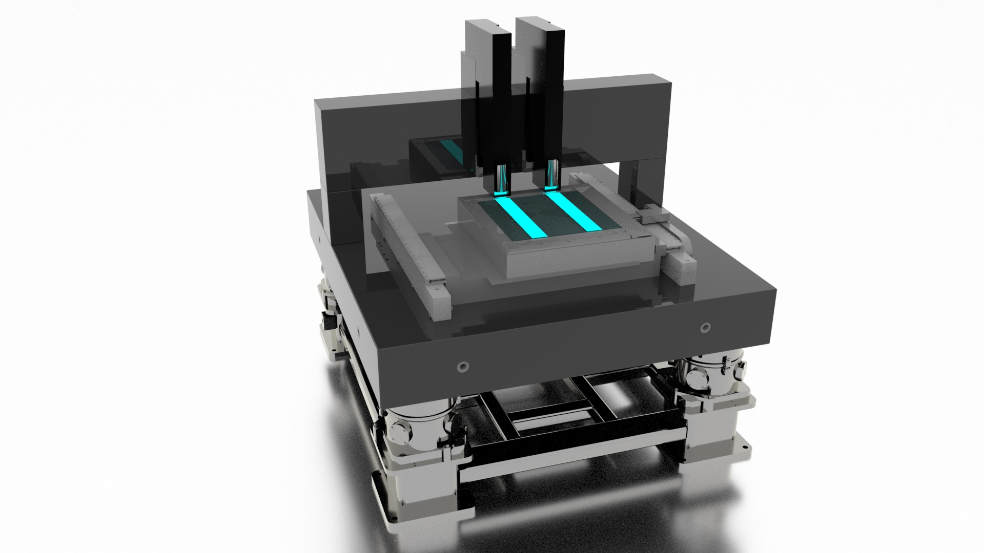
▲어플라이드 DLT 시스템(사진:어플라이드)
글라스·신소재 기반 대형 기판에 이종 칩렛
우시오 패키징용 리소그래피 기술력 결합
서브 마이크론 크기 배선으로 칩 조합 가능
AI 워크로드가 급격히 증가되면서 뛰어난 기능을 갖춘 반도체 칩 수요가 늘어나고 있다. 전통적인 무어의 법칙으로 감당할 수 없는 수준의 AI 미세화가 요구되면서 반도체 제조사들은 모놀리식(monolithic) 칩과 동일하거나, 그 이상의 성능 및 대역폭을 제공하기 위해 최첨단 패키지에 여러 칩렛을 통합하는 이종접합(Heterogeneous Integration) 제조 기술을 적극 채택하고 있다.
재료공학 솔루션 분야 글로벌 선도 기업 어플라이드 머티어리얼즈가 우시오(Ushio)와 전략적 파트너십을 맺고 3D 패키지에 칩렛을 이종접합 제조하는 업계 로드맵을 가속화한다고 4일 밝혔다.
이번 파트너십으로 인공지능(AI) 컴퓨팅 시대 필요한 최첨단 기판 패터닝에 특화 설계된 디지털 리소그래피 시스템이 함께 출시된다.
반도체 업계는 초미세 인터커넥트 피치와 탁월한 전기·기계적 특성 구현할 수 있는 글라스와 같은 신소재 기반의 대형 패키지 기판을 필요로 한다. 패널 가공 분야에 기술력을 가진 어플라이드와 패키징용 리소그래피 분야의 우시오가 이번 파트너십을 통해 이종접합으로의 패러다임 전환을 촉진할 것으로 기대했다.
새로운 디지털 리소그래피 기술(DLT) 시스템은 최첨단 기판 애플리케이션에 필요한 분해능을 구현하고 대량 생산에 요구되는 처리량을 제공하는 기술이다. 선폭 2마이크로미터(µm) 미만 배선 패터닝이 가능한 DLT 시스템을 활용하면 반도체 제조사는 웨이퍼, 글라스 및 유기소재로 제작된 대형 패널 등 모든 종류의 기판에 칩렛 아키텍처를 구현할 수 있다.
 ▲어플라이드 DLT 시스템(사진:어플라이드)
DLT 시스템은 예기치 못한 기판 휨 문제를 해결하고 오버레이 정확도를 제공하기 위해 특별히 설계됐다. 이미 많은 고객사에 생산 시스템이 납품됐고, 글라스 기판 포함한 다양한 최첨단 패키지 기판에 2µm 패터닝이 성공적으로 구현됐다.
어플라이드는 DLT 시스템 기반 기술을 개척했으며 우시오와 협력을 통해 1µm 이하 최첨단 패키징 선폭을 위한 연구개발을 지속하고 확장할 계획이다. 우시오는 풍부한 제조 기술 및 대면 고객 인프라를 활용해 DLT 도입을 가속화를 도모했다.
순다르 라마무르티(Sundar Ramamurthy) 어플라이드 이종접합·ICAPS·에피택시·반도체 제품 그룹 부사장 겸 총괄매니저는 “어플라이드의 새로운 DLT은 고객의 최첨단 기판 로드맵에 대한 니즈를 직접 해결하는 최초의 패터닝 시스템”이라며, “어플라이드는 대형 기판 가공에서의 독보적인 전문성, 업계에서 가장 폭넓은 이종접합 기술 포트폴리오, 풍부한 연구개발 자원을 적극 활용해 고성능 컴퓨팅의 차세대 혁신을 지원한다”고 말했다.
윌리엄 맥킨지(William F. Mackenzie) 우시오 광자 솔루션 글로벌 사업부 그룹 최고책임자 겸 총괄매니저는 “우시오는 약 20년 동안 패키징 애플리케이션에 필요한 리소그래피 시스템을 구축하고 전 세계 4천여개 툴을 제공했다”며 “새로 체결된 파트너십에 따라 우시오는 확장성 높은 제조 생태계와 탄탄한 현장 서비스 인프라를 통해 DLT 도입을 촉진하고, 급속도로 전개되는 패키징 기술 분야의 당면과제를 해결하기 위해 포트폴리오를 확장할 것”이라고 전했다.