기사입력 2024.08.07 14:22
반도체 및 고급 WLP(Wafer-Level Packaging) 애플리케이션용 웨이퍼 처리 솔루션의 선도 기업인 ACM 리서치(ACM Research, Inc.)가 창사 이래 최대의 습식 벤치 장비 수주를 기록했다.
2022-02-24 오후 5:02:12by 배종인 기자
ACM 리서치(ACM Research)가 고속 전기도금 장비 ‘Ultra ECP ap’의 대량 공급 계약 체결에 성공했다.
2022-05-19 오전 8:29:10by 배종인 기자
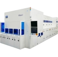
글로벌 장비 공급망의 리드타임이 증가하는 가운데 ACM 리서치가 포스트 CMP 세정 신제품을 출시하며 세정 장비 포트폴리오를 확장해 나가고 있다.
2022-08-11 오전 11:28:33by 권신혁 기자
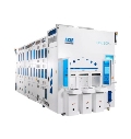
열 원자층 증착(thermal ALD)은 최신 노드 공정에서 빠르게 성장하는 기술로 로직 노드가 축소됨에 따라 반도체 제조사는 고급 공정에 필요한 최신 장비 수급에 열을 올리고 있다. 이러한 가운데 ACM 리서치에서 고급 공정 장비를 출하하며 기술력을 과시했다.
2022-10-14 오후 2:06:09by 권신혁 기자
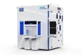
반도체 및 첨단 웨이퍼 레벨 패키징(WLP) 애플리케이션을 위한 웨이퍼 처리 솔루션 전문 기업인 ACM 리서치(ACM Research, Inc.)가 반도체 트랙 시장에 진출하며, 반도체 IC 제조용 리소그래피 지원에 나섰다.
2022-11-25 오전 11:36:55by 배종인 기자
.jpg)
반도체 및 첨단 웨이퍼 레벨 패키징(WLP) 애플리케이션을 위한 웨이퍼 처리 솔루션 전문 기업인 ACM 리서치(ACM Research, Inc.)가 SiC기판 세정용 Ultra C 장비의 첫 번째 구매 주문을 획득하며, 전력 반도체 시장에 진입했다.
2023-04-21 오전 11:17:12by 배종인 기자
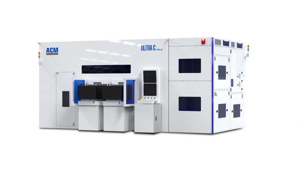
반도체 및 첨단 웨이퍼 레벨 패키징(WLP) 애플리케이션을 위한 웨이퍼 처리 솔루션 전문 기업인 ACM 리서치(ACM Research)가 새로운 진공 세정 솔루션을 발표하며, 첨단 3D 패키지의 새로운 세정 요구 사항을 충족 시켰다.
2023-09-27 오전 10:32:33by 배종인 기자

[열린보도원칙] 당 매체는 독자와 취재원 등 뉴스이용자의 권리 보장을 위해 반론이나 정정보도, 추후보도를 요청할 수 있는 창구를 열어두고 있음을 알려드립니다.
고충처리인 장은성 070-4699-5321 , news@e4ds.com


