기사입력 2024.10.09 05:03
한국재료연구원(KIMS, 원장 최철진)이 과학기술정보통신부가 출범한 ‘국가 수소 중점연구실’의 5대 분야 중 하나인 ‘음이온교환막 수전해’ 총괄주관 연구기관으로 지정됐다.
2024-07-24 오전 11:20:50by 배종인 기자
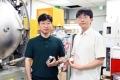
한국전기연구원(KERI) 차세대전지연구센터 하윤철 박사팀이 경희대 응용화학과 김병곤 교수팀, 중앙대 에너지시스템공학부 문장혁 교수팀, 부산대 재료공학부 이승기 교수팀과 함께 전고체전지(황화물계)용 양극활물질과 고체전해질을 최적으로 혼합할 수 있는 기술을 개발했다.
2024-07-29 오후 1:23:14by 배종인 기자
.jpg)
한국재료연구원(KIMS, 원장 최철진)과 한국기계연구원(KIMM, 원장 류석현)이 연구 협력을 위한 ‘협력마중물 사업’의 원활한 소통의 자리인 ‘2024년 기계연-재료연 1차 협력교류회’를 개최했다.
2024-07-29 오후 3:10:20by 배종인 기자
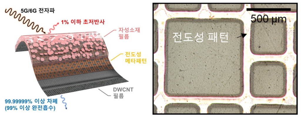
한국재료연구원(KIMS, 원장 최철진) 나노재료연구본부 김경태 박사 연구팀이 원자 규모의 결함을 인위적으로 형성한 비스무트 텔루라이드(Bi-Te)계 열전반도체 재료를 개발하고, 버려지는 열에너지를 활용하기 위한 물성 향상 솔루션을 제시하며, 수십년간 정체됐던 n형 열전반도체 연구의 돌파구가 마련될 것으로 기대된다.
2024-08-07 오전 11:38:50by 배종인 기자
.jpg)
한국재료연구원(KIMS, 원장 최철진)이 지난 3년간 국가 소재산업 기업지원을 위해 핵심 역할을 수행하며, 소재 기업들의 성장 기반 강화에 크게 이바지했다.
2024-08-08 오후 4:31:10by 배종인 기자
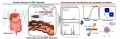
한국재료연구원(KIMS, 원장 최철진) 바이오·헬스재료연구본부 정호상 박사 연구팀이 침, 점액, 소변 등 체액 내 암 대사체의 광신호를 증폭하고, 이를 인공지능으로 분석해 암을 진단하는 혁신적인 센서 소재를 개발했다.
2024-08-12 오전 9:43:43by 배종인 기자
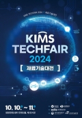
한국재료연구원(KIMS, 원장 최철진)이 10월10일부터 11일까지 창원컨벤션센터(CECO)에서 국내 소재부품 기업 관계자들을 대상으로 ‘KIMS TECHFAIR 2024’를 개최한다.
2024-10-07 오후 1:57:02by 배종인 기자

[열린보도원칙] 당 매체는 독자와 취재원 등 뉴스이용자의 권리 보장을 위해 반론이나 정정보도, 추후보도를 요청할 수 있는 창구를 열어두고 있음을 알려드립니다.
고충처리인 장은성 070-4699-5321 , news@e4ds.com