

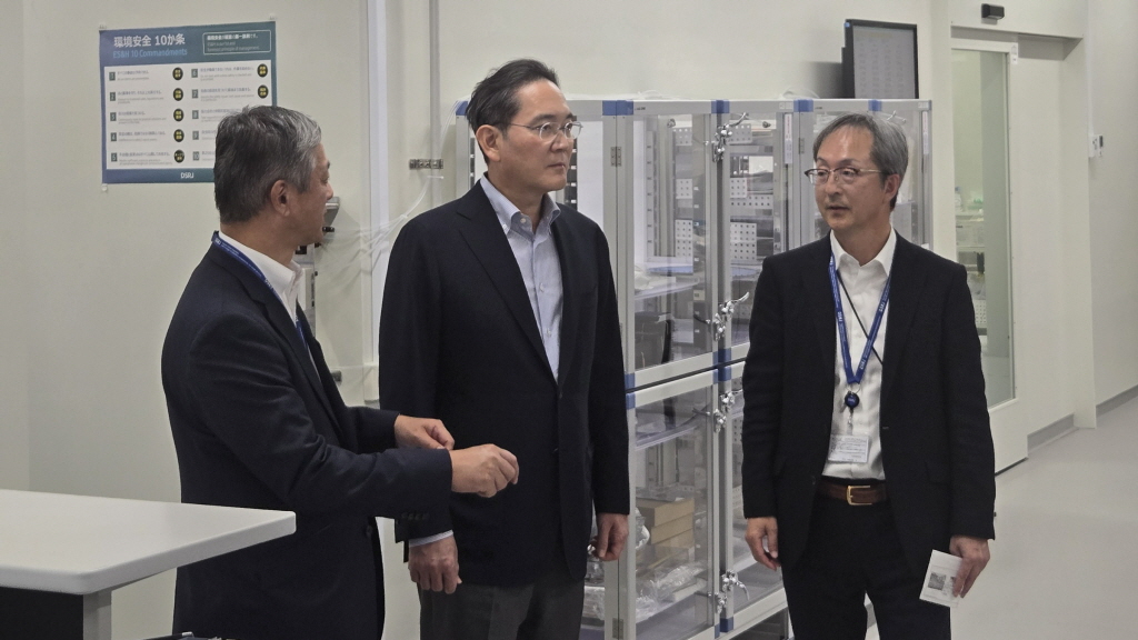
Chairman Lee Jae-yong Inspects Advanced Packaging…Visits Yokohama APL in Japan
Samsung Electronics Chairman Lee Jae-yong visited the 'Advanced Package Lab (APL)', an advanced semiconductor packaging research hub in Yokohama, Japa…
2026.11.02 by 배종인 기자
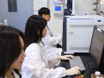
KBG expands high-purity silicon business for semiconductor packaging with low-volatility silicon technology
KBG, a functional silicon material company, has established a process to remove low-molecular siloxanes to 150ppm or below using thin film evaporator …
2026.10.13 by 배종인 기자

Henkel to Unveil Advanced Packaging Materials for AI and HBM at SEDEX 2026
Henkel will showcase semiconductor high-density packaging solutions for the AI and HBM era at SEDEX 2026. Through advanced materials such as underfill…
2026.10.06 by 배종인 기자
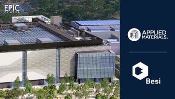
Applied Materials and Besi Expand AI Packaging Partnership
Applied Materials and Besi are expanding their strategic partnership to respond to growing demand for highly integrated semiconductor packaging driven…
2026.10.02 by 배종인 기자

Applied Materials Acquires NEXX… Expanding Panel-Based Advanced Packaging Capabilities
Applied Materials has entered into a contract to acquire ASMPT's NEXX business division. This acquisition is interpreted as a strategic move to expand…
2026.05.07 by 배종인 기자