2.5D 및 3D 집적 기술은 첨단 반도체의 수율 문제 해결을 위해 고안됐다. 그리고 그 효용은 TSMC가 자일링스의 FPGA를 CoWoS 기술로 양산함으로서 입증했다. 이에 착안한 인텔은 포베로스 기술을 개발하여 자사의 CPU 성능을 높였다. 국내 시스템 반도체 산업이 TSMC와 인텔을 극복하려면 기존의 패키징 기술에 대한 관점을 부정하는 파괴적인 혁신이 필요하다.
2.5D 집적, 첨단 반도체 수율 문제 해결의 열쇠
인텔 포베로스, TSMC CoWoS 기술이 대표적
웨이퍼 레벨의 첨단 패키징 공정이 필요한 때
모든 산업에서 AI 기술의 중요성이 높아지며 AI 프로세스를 전문적으로 처리하는 AI 반도체에 관한 관심이 뜨겁다. 우리 정부 역시 이달 10일, AI 반도체 개발에 10년에 걸쳐 1조96억 원을 투입하겠다고 밝혔다. 이는 최근 5년간 진행된 R&D 사업 중 최대 규모다.
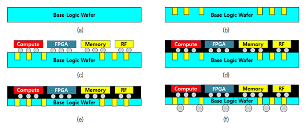
▲ 미세 공정에서 제작되는 반도체의 수율을 높이기
위해서는 2.5D 및 3D 패키징 기술이 필요하다
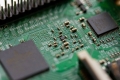
각종 반도체 중에서도 최첨단을 달리는 AI 반도체를 설계하고 생산하는 일은 간단치가 않다.
미국의 컨설팅 업체인 IBS에 따르면, 일반적으로 반도체 설계비용은 28㎚ 평면 디바이스의 경우 5,130만 달러다. 비용은 7㎚에서는 2억9,780만 달러, 5㎚에서는 5억4,220만 달러로 급증한다. 3㎚에서는 최소 5억에서 최대 15억 달러에 이른다.
거액의 돈을 투자해 반도체를 설계했다 하더라도 이를 적당한 수율로 생산할 수 있는 파운드리는 대만의 TSMC, 우리나라의 삼성전자, 미국의 인텔뿐이다. 이들 역시 수율을 유지하고 높이기 위해서 매년 천문학적인 돈을 투자하고 있다.
한국전자통신연구원(ETRI)의 최광성 책임연구원은 2.5D 집적 기술과 3D 집적 기술이 AI 반도체를 비롯한 첨단 반도체의 수율 문제를 해결하기 위해 고안되었다고 ‘인공지능 모듈용 2.5D/3D 집적 기술 개발 동향’을 통해 설명했다.
2.5D 집적 기술은 실리콘 관통 전극(Through Silicon Via; TSV)을 가진 실리콘 인터포저(Interposer)에 디바이스를 뒤집어서 붙이는, 즉 플립 칩 본딩(Flip Chip Bonding)을 하여 집적도를 높이는 기술이다.
3D 집적 기술은 디바이스 자체에 TSV를 형성하여 이를 3차원으로 집적하는 기술이다. 현재 삼성전자, SK하이닉스가 이 기술을 적용하여 HBM(High Bandwidth Memory)을 양산하고 있다.
◇ 2.5D 집적, 반도체 수율 높이는 가장 현실적인 방법
최광성 연구원은 2.5D 집적 기술과 첨단 반도체 공정 수율의 연관성이 2012년, TSMC가 자일링스의 FPGA를 2.5D 집적 기술로 양산하며 증명됐다며 관련 내용을 소개했다.
당시의 FPGA는 28㎚ 기술로 제조됐다. 문제는 수율이었고, 수율을 떨어뜨리는 원인은 큰 칩 크기였다. 이를 해결하기 위해 칩을 분리하는 방안이 등장했다. 하나의 칩을 네 조각으로 분리하는 것이었다.
분리된 칩들이 하나의 칩으로 동작하기 위해서는 새로운 부품, 실리콘 인터포저가 필요했다. 이는 분리된 개별 칩들의 기판과의 접합을 위한 범프 수가 약 5만 개, 피치는 약 45㎛였고, 이들 범프를 연결하기 위한 배선의 최소 폭이 0.5㎛로 매우 얇았기 때문이다.
최 연구원은 “2.5D 집적 기술에서 채용된 실리콘 인터포저는 고밀도의 범프를 갖는 높은 성능의 칩을 기판과 물리적으로 연결할 수 있는 현실적인 방법을 제시한 것이다”라며, “이러한 기술적인 전환은 반도체 공정 노드가 미세해질수록 발생하는 비용 문제에 대해서 지금까지도 통하는 해법을 제시한다”라고 평했다.
치플렛(Chiplet)이라는 단위 IP 블록을 다양한 반도체 공정 노드에서 제조하고, 이를 실리콘 인터포저에 집적하여 전체적인 비용을 절감하는 치플렛 집적(Chiplet integration) 기술이 그 사례다.
◇ 웨이퍼 단위 통합 공정으로 수율을 높인 인텔
2020년 6월, 인텔은 ‘포베로스(Foveros)’라는 패키징 기술로 개발한 ‘레이크필드(Lakefield)’라는 코드명의 랩톱용 CPU를 시장에 선보였다. 인텔은 해당 프로세서가 단일 칩을 사용한 전 세대 프로세서보다 성능이 12% 높고, 대기전력이 92% 적고, 전체적인 전력 효율이 24% 높다고 밝혔다.
▲ 포베로스 공정 개략도 [그림=ETRI]
포베로스는 3차원 패키징 기술로, 로직 웨이퍼를 완성한 다음 TSV를 형성한다. 그 후 다양한 반도체 공정 노드에서 나온 디바이스를 C2W(chip-to-wafer) 공정으로 접합하고, 웨이퍼 레벨 몰딩 공정을 하고 그라인딩 공정을 통해 접합된 칩들의 상면을 드러내어 방열 대책을 세운다.
다음으로 로직 웨이퍼 아랫면을 그라인딩 및 폴리싱하여 TSV를 드러내고 후면 배선 공정과 솔더 범프를 형성한다. 마지막으로 웨이퍼를 개별 칩으로 분리한 다음 HBM 등이 있는 기판에 집적하면 레이크필드 프로세서가 완성된다.
최 연구원은 이러한 공정은 기존 패키징 공정과 몇몇 부분에서 차별화된다고 설명했다.
첫 번째는, 패키징 기술과 팹 공정의 혼합이다. 기존에는 팹 공정과 패키징 공정을 명확하게 전공정, 후공정으로 구분할 수 있었다. 그러나 포베로스에서는 TSV 형성 공정, 접합 공정, 몰딩 공정이 혼합되어 팹 공정과 패키징 공정 구분이 무의미해졌다.
두 번째는, 기판으로 값비싼 로직 웨이퍼가 적용되었다는 점이다. 세 번째는, 모든 공정이 웨이퍼 단위에서 진행된다는 점이다.
◇ 2.5D 집적, 웨이퍼 레벨 불량에 대한 공포 극복해야
최 연구원은 시스템 반도체를 위한 2.5D 집적 기술이 TSMC로부터 시작되었다고 말했다. TSMC의 CoWoS(Chip-on-Wafer-on-Substrate) 기술의 개념은 인텔의 포베로스 기술과 유사하다.
단, 로직과 같은 디바이스를 기판으로 사용하는 것이 아니라 TSV 실리콘 인터포저를 기판으로 사용한다는 점에서 차이가 있다. 그 외 C2W 본딩, 웨이퍼 레벨 몰딩, 실리콘 그라인딩 및 폴리싱을 통한 TSV 노출 등의 공정은 CoWoS에서 이미 선보인 기술이다.
최 연구원은 “지금도 그렇지만 당시에 TSV 실리콘 인터포저 제조 시 가장 어려운 공정 중 하나는 직경 300㎜, 두께 약 100㎛의 TSV 실리콘 인터포저를 공정 중에 혹은 공정 간 이동 중에 취급하는 것”이라 말했다. 쉽게 깨지기 때문이다.
이 문제를 해결하기 위해 전 세계의 소재 및 공정 회사들이 다양한 기술을 제안했다. TSMC는 취급하고자 하는 TSV 실리콘 인터포저의 두께를 두껍게 해서, 그것도 패키징 공정 중에 하나의 공정인 본딩 기술과 몰딩 기술을 적용하여 해결하였다. 이 아이디어는 웨이퍼 레벨 불량이 발생할 경우의 손실에 대한 공포를 극복했기 때문에 구현될 수 있었다.
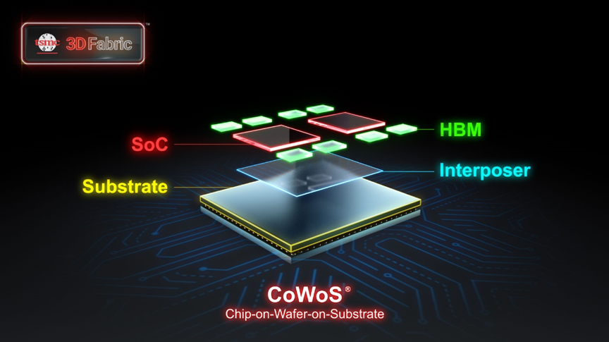
▲ CoWoS 기술 [그림=TSMC]
최 연구원은 우리나라에서도 웨이퍼 레벨의 첨단 패키징 공정에 대한 많은 시도가 있었지만, 한 공정에서라도 불량이 발생하면 다량으로 발생할 우려가 크고, 값비싼 디바이스를 버리는 손실이 너무 클 것이라는 고정관념으로 인해 이를 적용하기 어려운 분위기가 지금도 팽배한다고 지적했다.
그러면서 국내 파운드리는 여전히 “반도체 공정을 전공정-후공정으로 나누고, 대부분의 부가가치는 전공정에서 나오므로 후공정은 수율만 올리면 된다는 고정관념이 웨어퍼 레벨 공정을 국내에서 구현되지 못 하게 하고 있다”라고 비판했다.
◇ 기존 패키징 기술을 뛰어넘는 파괴적인 혁신 필요
AI 모듈의 핵심 부품인 3차원 적층 메모리, 즉 HBM은 국내 기업인 삼성전자와 SK하이닉스가 주로 제작하고 있다. 양사의 HBM은 다음과 같은 과정을 거쳐 만들어진다.
메모리 소자를 먼저 만든 후, TSV를 형성한 뒤, BEOL(Back End Of Line)과 재배선, 그리고 범프를 제작한다. 그 후 캐리어 웨이퍼에 임시 접합을 한 다음 TSV를 드러내고, 후면 재배선과 범프를 제작한다. 이 웨이퍼를 캐리어 웨이퍼에서 분리한 다음 마스터 메모리에 적층 공정을 실시한다.
인텔의 포베로스, TSMC의 CoWos와 다른 점은 마스터 메모리가 TSV가 완성된 반제품이라는 사실이다. 마스터 메모리의 두께가 약 50㎛밖에 되지 않아 캐리어 웨이퍼에 임시 접합되어 있다. 최 연구원은 HBM 제작 공정을 보면 전통적인 전공정과 후공정으로 제조공정이 나뉘어져 있다고 지적했다.
최 연구원은 “우리나라의 시스템 반도체 산업이 TSMC와 인텔을 극복하려면 기존의 패키징 기술에 대한 관점을 부정하는 파괴적인 혁신이 필요하다”라며, “패키징 기술을 반도체 전공정 이후의 후공정이 아닌 새로운 부가가치 창출과 시장의 요구를 만족시키는 혁신 기술의 주체로 관점을 바꾸어야 한다”라고 조언했다.
.jpg)