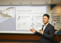
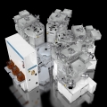
어플라이드 머티어리얼즈가 기존대비 30% 더 적은 공간에서 생산성을 더욱 극대화한 새로운 식각 솔루션인 ‘비스타라(Vistara)’ 플랫폼을 출시하며, 생산 수율 및 지속가능성 등에서 고민하던 반도체 메이커들의 생산 문제를 해결했다.
모듈식 아키텍처 12개까지 챔버 구성, 타사 챔버 사용 可
방대한 데이터 확인 센서 수천개, 챔버 전체 일관성 유지
어플라이드 머티어리얼즈가 기존대비 30% 더 적은 공간에서 생산성을 더욱 극대화한 새로운 식각 솔루션을 출시하며, 생산 수율 및 지속가능성 등에서 고민하던 반도체 메이커들의 생산 문제를 해결했다.
어플라이드는 30일 기자간담회를 통해 최근 출시한 새로운 웨이퍼 생산 플랫폼인 ‘비스타라’를 소개하는 자리를 가졌다.
이날 소개된 비스타라(Vistara)는 최근 반도체 메이커들이 안고 있는 고민인 △2D에서 3D 구조로 변화하며 4배 이상 증대된 복잡성 △ 단위 면적당 산출량에 대한 비용 증가 △로드 투 로드의 변경으로 인한 시간 증대 △에너지 소비량 증가로 인한 탄소 배출문제 등에 있어서 유연성, 인텔리전스, 지속가능성을 제공해 앞서 언급한 반도체 생산 문제 해결을 지원할 것으로 기대된다.
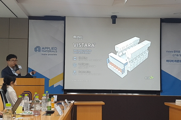
▲장대현 메모리 식각 기술 총괄이 ‘비스타라(Vistara)’ 플랫폼을 소개하고 있다.
비스타라는 모듈식 아키텍처를 채택해 최소 4개에서 최대 12개까지 챔버를 구성할 수 있고, 타사 챔버와 같이 사용해 새로운 종류의 진공 통합 솔루션을 만들 수도 있다.
이에 고객에게 통합재료 솔루션, 생산성 및 설치 공간에 대한 유연성을 제공한다.
또한 실시간 제어 데이터를 제공하는 수천개의 센서가 포함돼 있고, AIx 플랫폼을 포함한 응용소프트웨어는 이 데이터를 사용해 고객이 장비 및 챔버간 매칭 그리고 유지 보수 후 착수 기간을 획기적으로 줄여서 연구개발을 가속화할 수 있도록 지원한다.
여기에 설계 및 소프트웨어 인텔리전스를 사용해 펌프 및 환기 시간을 동적으로 최적화함으로써 칩제조업체가 결함을 줄여 수율을 극대화하도록 돕는다.
반도체 업계의 화두인 지속가능성 문제도 크게 향상시켰다. 어플라이드는 가스패널을 재설계함으로써 비스타라 플랫폼이 펌프, 열교환기, 냉각기를 포함한 서브팹 구성요소를 사용하는 방식을 최적화했다.
이러한 개선사항은 이전 플랫폼 대비 에너지소비를 최대 35%를 줄여 칩제조업체가 스콥1(직접 탄소배출량) 및 스콥2(간접 탄소배출량) 온실가스 배출량을 줄이는데 도움이 된다.
비스타라 사용시 칩제조업체는 평방피트당 더 많은 시스템을 설치해 클린룸 공간을 최대화 할 수 있도록 했다.
비스타라는 12개의 식각챔버를 통합해 기존 2개의 센드리스 플랫폼의 동일한 생산성을 30% 더 적은 공간에서 제공한다.
새로운 팹을 건설할 때 칩제조업체는 더 작은 클린룸에서 목표 웨이퍼 생산량을 달성할 수 있고 팹건설 중에 사용되는 에너지의 양도 감소시킬 수 있다.
여기에 어플라이드의 새로운 에코 트윈소프트웨어가 함께 제공돼 칩제조업체가 추가적인 환경절약을 위해 프로세스 레시피의 에너지 및 재료 소비를 모니터링하고 최적화하는데 도움을 준다.
발표를 담당한 장대현 메모리 식각 기술 총괄은 “비스타라는 지속가능성의 대표적인 플랫폼으로 화학물질 사용량을 30% 절감할 수 있고, 소재 사용량도 절감할 수 있다며, 칩 제조 유연성, 인텔리전스 및 지속가능성의 궁극적인 반도체 솔루션”이라고 전했다.
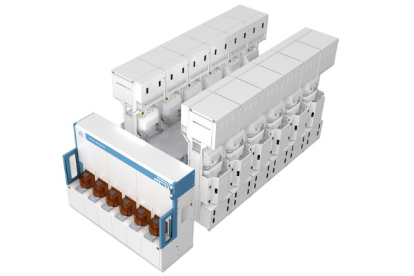
▲‘비스타라(Vistara)’ 플랫폼
한편 이날 발표에서는 소비전력을 크게 줄일 수 있는 이종칩 결합에 대한 어플라이드 머티어리얼즈의 솔루션도 발표됐다.
발표를 담당한 박흥락 패키지 기술 총괄은 하이브리드 본딩과 실리콘관통전극 공법을 사용해 칩렛을 최신 2.5D 및 3D 패키지에 통합하는데 도움이 되는 재료, 기술, 신제품을 소개했다.
박흥락 총괄은 지금의 기술로는 향후 슈퍼컴퓨터 2대를 가동하는데 원자력 발전소 한기의 전력을 소모하는 시대가 올 것이라며 이를 해결하기 위해서는 반도체 소비전력을 줄여야 하고, 이종 접합 제조(Hi, Heterogeneous Integration)를 통해 반도체 회사가 다양한 기능, 기술노드, 크기의 칩렛을 최신 패키지로 결합해 단일 제품처럼 작동하게 한다면 소요되는 소비전력을 급격하게 줄일 수 있다고 밝혔다.
이를 위해 어플라이드는 PPACt(전력, 성능, 크기, 비용, 시장 출시기간)을 개선하도록 칩 투 웨이퍼(Chip-to-wafer), 웨이퍼 투 웨이퍼(wafer-to-wafer) 하이브리드 본딩을 통해 구리-구리 결합을 이용해 직접 칩들을 연결함으로써 결합된 소자들이 단일 소자처럼 성능을 내도록 돕는다.
이를 구현하는 장비들로는 인세프라(Insepra) SiCN 증착 시스템, 카탈리스트(Catalyst) CMP 솔루션 등이 있다.
또한 여기에 실리콘에 트렌치를 식각한 다음 절연막과 금속 배선으로 적층된 칩을 정밀하게 연결해 주는 수직 배선인 TSV를 구현하기 위해서 어플라이드는 △프로듀서 인비아 2(Producer InVia 2) △엔듀라 벤튜라 2(Endura Ventura 2) PVD 시스템 △프로듀서 아빌라(Producer Avila) PECVD 시스템 등도 공급하고 있다.