기사입력 2024.05.02 15:07

UNIST(총장 이용훈) 에너지화학공학과 곽원진 교수팀이 한양대 기계공학과 최준명 교수팀과 공동으로 유기 전극의 장점을 유지하면서 획기적으로 전지의 성능을 향상시킬 수 있는 전해질을 개발했다.
2024-02-01 오후 4:22:09by 배종인 기자
UNIST(총장 이용훈)는 현대자동차(대표이사 이동석)와 울산시 남구 두왕동 UNIST 산학융합캠퍼스 내 3D프린팅 융합기술센터에서 ‘3D프린팅 공동 연구개발실 운영을 위한 상호 협력 약정’을 체결했다.
2024-02-05 오후 3:01:39by 배종인 기자

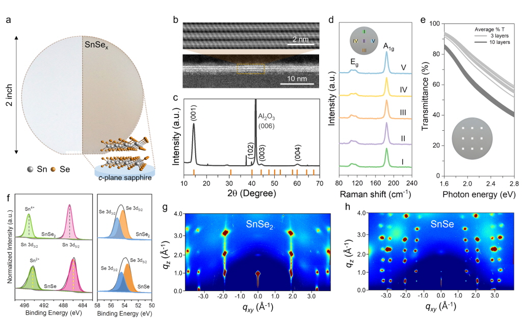
UNIST(총장 이용훈) 신소재공학과 김지윤 교수팀이 기존의 재료의 한계를 뛰어넘어 실시간으로 물질의 모양과 특성을 조절할 수 있는 메타 물질을 세계 최초로 개발했다.
2024-02-05 오후 3:05:29by 배종인 기자
UNIST(총장 이용훈) 화학과 오현철 교수는 보통의 대기압에서도 수소를 고밀도로 저장할 수 있는 나노다공성 수소화붕소마그네슘 구조(Mg(BH4)2)를 보고했다.
2024-02-13 오후 2:14:28by 배종인 기자
UNIST(총장 이용훈) 화학과 조재흥 교수팀이 산화력이 뛰어난 새로운 망간-플루오린 촉매 합성에 성공했다.
2024-02-21 오전 11:50:00by 배종인 기자
기초과학연구원(IBS, 원장 노도영) 나노입자 연구단 김대형 부연구단장(서울대 화학생물공학부 교수)과 현택환 단장(서울대 화학생물공학부 석좌교수) 연구팀은 최문기 UNIST 교수, 양지웅 DGIST 교수팀과 공동으로 세계 최고 성능의 스트레처블 QLED(퀀텀닷발광다이오드) 개발에 성공했다.
2024-04-16 오전 9:44:12by 배종인 기자
.jpg)
UNIST(총장 이용훈) 에너지화학공학과 장지욱, 장성연 교수팀은 스탠퍼드 대학교 Thomas F. Jaramillo 교수와 공동으로 페로브스카이트 기반 친환경 암모니아 생산 광전극 시스템을 개발했다. 이 기술을 이용하면 태양에너지만으로 고효율의 암모니아를 생산할 수 있을 것으로 기대된다.
2024-04-16 오후 4:03:06by 배종인 기자

[열린보도원칙] 당 매체는 독자와 취재원 등 뉴스이용자의 권리 보장을 위해 반론이나 정정보도, 추후보도를 요청할 수 있는 창구를 열어두고 있음을 알려드립니다.
고충처리인 장은성 070-4699-5321 , news@e4ds.com