기사입력 2024.09.13 10:17
.jpg)
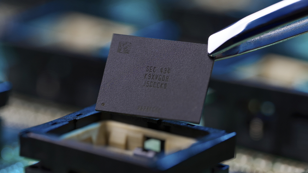
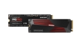
삼성전자가 SAS-4 표준을 지원하는 서버용 SSD, PM1653를 출시했다. PM1653은 6세대 V낸드가 처음 적용된 초고속 엔터프라이즈 서버 전용 제품으로, 800GB부터 최대 30.72TB까지 고객 수요에 맞춰 다양한 용량으로 출시한다.
2021-04-28 오전 8:12:33by 강정규 기자
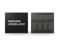
삼성전자가 D램과 낸드플래시 메모리를 한 칩에 담은 최고 성능의 uMCP 신제품 출시를 통해 스마트폰 제조사들의 디자인 편의성과 공간 활용성을 높였다.
2021-06-15 오후 4:48:03by 배종인 기자
[편집자주] 반도체 업계 낸드플래시 적층이 200단을 넘어섰다. 싱글 스택으로 128단을 쌓은 삼성전자 외에는 200단을 넘기 힘들 거라던 지난 말들이 무색하게 적층 경쟁에서 선두에 선 것은 다름아닌 232단을 쌓아 올린 미국의 마이크론이었다. SK하이닉스가 이에 질세라 238단 낸드 플래시 상용화를 예고하며 200단대 선두 싸움에 뛰어들었다. 삼성은 올 초 172단 7세대 V낸드를 UFS 4.0에 탑재하며 관망하는 모양새지만 200단대 기술 확보는 이미 완료됐다며 자신감을 내비쳤다. 200단 낸드 시대, 반도체 제조사들의 격돌을 살펴봤다.
2022-08-12 오후 1:00:42by 권신혁 기자
“삼성전자가 약 40년간 만들어낸 메모리의 총 저장용량이 1조 기가바이트(GB)를 넘어서고, 이중 절반이 최근 3년간 만들어졌을 만큼 우리는 급변하는 디지털 전환을 체감하고 있다”
2022-10-07 오전 10:10:35by 권신혁 기자
.jpg)
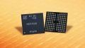
삼성전자가 웨이퍼당 비트 집적도를 대폭 향상시킨 세계 최고 용량의 8세대 V낸드 양산에 들어가며, 차세대 서버 시장의 고용량화 주도와 함께 고신뢰성을 요구하는 전장 시장까지 V낸드 사업 영역을 확대한다.
2022-11-07 오후 2:13:28by 배종인 기자
삼성전자가 최첨단 8세대 V낸드가 적용되고, PCle 4.0 기반 소비자용 SSD 중 가장 빠른 임의 읽기 속도 제공하는 고성능 SSD를 출시하며 고성능 게임, 3D/4K 그래픽 작업을 전문으로 하는 소비자 공략에 나선다.
2023-09-12 오전 8:56:13by 배종인 기자
삼성전자가 더블 스택 구조로 구현 가능한 최고 단수를 쌓은 ‘1Tb(테라비트) TLC(Triple Level Cell) 9세대 V낸드’ 양산을 시작하며, 메모리 반도체 기술 리더십을 증명했다.
2024-04-23 오후 4:13:06by 배종인 기자

[열린보도원칙] 당 매체는 독자와 취재원 등 뉴스이용자의 권리 보장을 위해 반론이나 정정보도, 추후보도를 요청할 수 있는 창구를 열어두고 있음을 알려드립니다.
고충처리인 장은성 070-4699-5321 , news@e4ds.com


