


2026 Intermediate Engineer Practical Master Class - Circuit Design Methods and Component Failure Causes and Prevention Measures
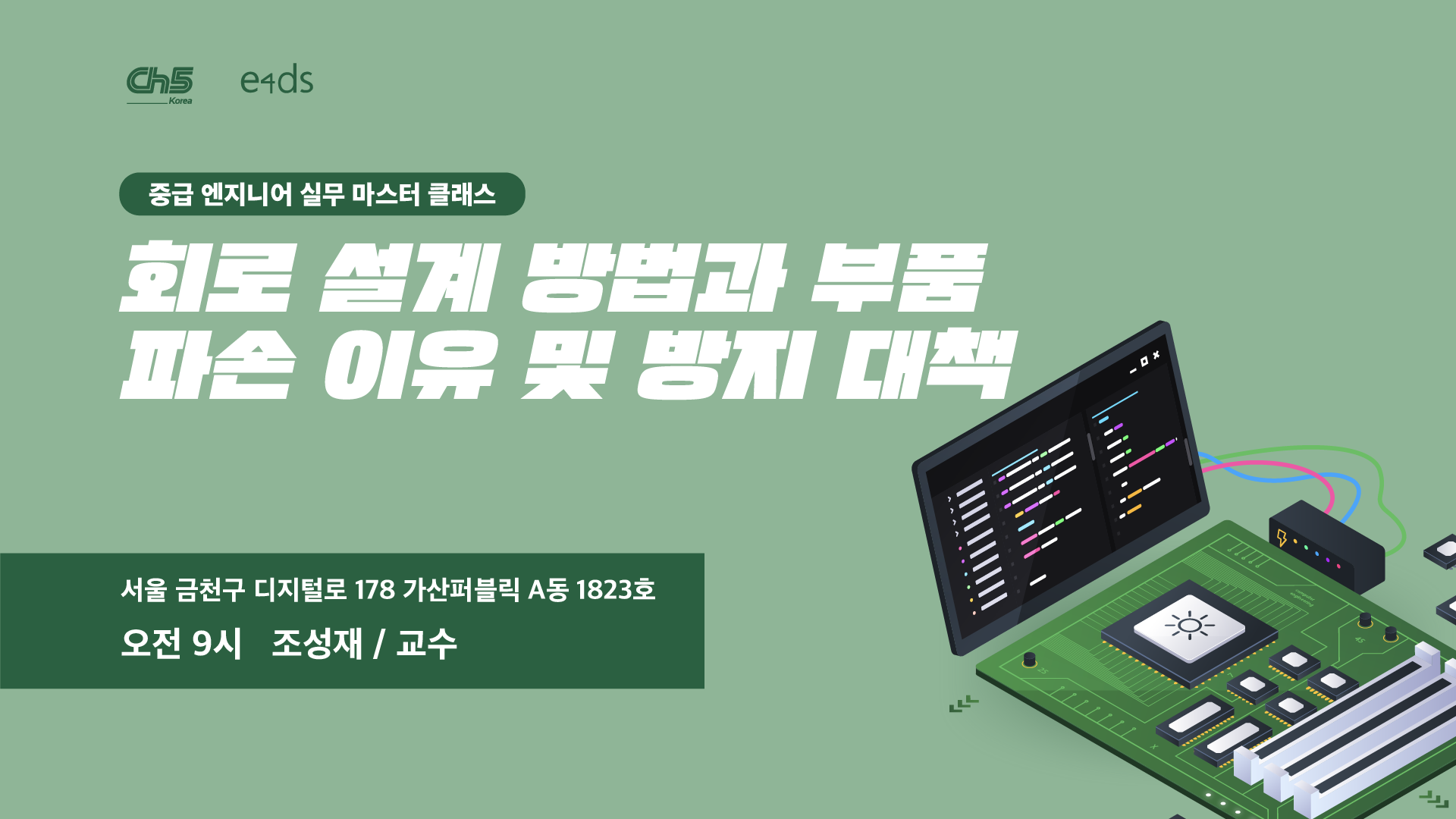
Venue: e4ds Conference Center
Address: 서울 금천구 디지털로 178 (가산동) 가산퍼블릭 A동 1823호
- This course is an offline paid hands-on training program, not an online broadcast lecture.
- Clicking the webinar registration button at the top will redirect you to the registration page.
- Please note that payment must be completed one week before the training date.
- Please note that the training schedule may be changed if the number of attendees is low.
- Q&A sessions may extend until 6:00 PM, so please take this into account when booking public transportation.
Course Overview and Objectives
This is an advanced training course targeting current developers and engineers with practical circuit design experience, covering advanced topics in electronic circuit design and real-world problems in precision measurement environments.
Based on 35 years of expertise from Professor Cho Sung-jae of the Department of Electrical and Electronic Engineering at Shinhan University,
Focusing on component failure cases that frequently occur in actual field practice, this course provides in-depth coverage of the operating principles and key design considerations for switching circuits, relay driving, diodes, transistor amplification, timer circuits, and negative power supply design.
<Detailed Course Content>
1. Switching Circuit Design
Develop a deep understanding of the structure and operating principles of switching circuits, and learn the problems that can occur in the design process and optimal conditions.
- Problems in switching circuit design using load lines
- Switching circuit design methods: optimal conditions
- Design considerations for switching circuits: understanding the relationship between load, switching speed, heat generation, and EMI noise
- Transistor circuit design
- FET circuit design
- Photo Coupler circuit design
- Component selection and component damage prevention methods
- Pattern design to reduce noise emissions in switching circuit implementation
Achieve a complete understanding of switching circuit principles, save unnecessary costs and time during the design phase, and ensure circuit stability.
2. Diode Circuit Design
Understand the electrical characteristics and failure causes of various diodes (Si, Schottky, SiC, GaN, etc.) commonly used in field practice, and learn proper design techniques based on this understanding.
- Key parameters in diode selection
- Diode types (Si, Schottky, SiC, GaN, etc.)
- Primary factors in diode failure: reverse voltage and peak current
- Malfunction effects in diode circuits: concept and importance of Trr
- Forward voltage, reverse voltage, leakage current, and Trr characteristics by diode type
- Component selection and damage prevention methods based on circuit operation
Develop a deep understanding of diode structure and operating characteristics to improve circuit durability and reliability.
3. Transistor Amplification Circuit Design
Starting from the limitations of load line design, learn various amplification circuit configurations step-by-step, including simple amplification circuits and buffer/feedback circuits.
- Problems in amplification circuit design using load lines
- Optimal design methods
- Simple video amplification circuit design methods
- Necessity of buffer circuits
- Feedback video amplification circuit design methods
- Low-noise amplification circuit design methods
- Causes of measurement errors in oscilloscope measurements
Develop a deep understanding of transistor amplification circuit principles and structure, and design optimized circuits according to your objectives.
4. Simple Negative Power Supply Generation Methods
Learn step-by-step from the basic principles of Negative Converters to negative power supply generation methods using clock, timer, and Charge Pump circuits.
- Negative Converter operating principles
- Principles of negative power supply generation using clocks
- Reasons for negative power supply generation using timers
- Operating principles of Charge Pump circuits
Acquire practical design techniques to implement negative power supplies with simple circuits without using SMPS.
5. OP AMP Circuit Design and Practical Problem Solving
Develop a deep understanding of the structural and electrical characteristics of OP AMP, and learn optimal circuit design methods that consider input/output problems occurring in field practice, malfunction causes, and field environmental variables.
- OP AMP selection criteria
- Understanding input/output ranges
- Three factors affecting output range
- Misconceptions about OP AMP output range (actual meaning of load)
- Sensitivity degradation causes when using single supply and circuit design precautions
- OP AMP circuit malfunction causes and design precautions
- Response to differences between development and field environments
Improve your understanding of OP AMP, quickly diagnose and resolve output limitation and sensitivity degradation problems that occur during practical circuit development, and significantly reduce design errors.
6. Differential Amplifier vs Instrumentation Amplifier
Compare the structural differences and operating principles of differential amplifiers and Instrumentation Amplifiers for processing low-noise, high-precision signals, and learn design methods to maximize Common Mode noise suppression performance.
- Principles of differential amplifiers and Instrumentation Amplifiers resistant to common mode noise
- Single-Ended vs Differential Signal
- Necessity and design tips for Instrumentation Amplifier
- Malfunction causes and precautions when designing Instrumentation Amplifier
Secure noise suppression capability required for high-precision measurement and control systems, and implement stable signal processing circuits resistant to real-world noise problems.
7. OP AMP Filter Circuit Design
Learn the operating principles and design procedures of 1st to 3rd order OP AMP-based Active Filters (LPF/HPF), and compare the differences between active filters and passive filter plus amplification combinations to master high-quality analog signal conditioning techniques.
- 1st, 2nd, and 3rd order Active LPF/HPF design
- Precautions when designing active filters
- Characteristics and performance comparison between (active filter) and (passive filter + amplification circuit)
- Importance of linear phase
Develop high-performance filter design capabilities for noise suppression and signal distortion minimization, and apply them to the analog preprocessing stage of various systems.
<Hands-on Training Equipment>
- Oscilloscope
- Function Generator
- Power Supply
Instructor: Professor Cho Sung-jae
- B.S. in Electronic Engineering, Kyungpook National University
- M.S. in Electrical and Electronic Engineering, KAIST
- Ph.D. coursework completed in Electrical and Electronic Engineering, KAIST
- 10 years of service at Samsung Electronics Advanced Institute of Technology
- Former Expert Committee Member, National Technical Qualification in Electronics
- Former Expert Committee Member for Master Craftsman Selection in Electronics, Republic of Korea
- Former Professor, Department of Electronic Engineering, Shinhan University
- Emeritus Professor, Department of Electronic Engineering, Shinhan University
Venue: e4ds Conference Center
Address: 서울 금천구 디지털로 178 (가산동) 가산퍼블릭 A동 1823호
지하철 : 가산 디지털 단지역 6번출구 도보 9분 버스 : 5537, 6004, 5615, 5616, 5618, 5619, 5626, 5630, 5712, 5714, 21광명, 75부천, 652, 653, 5012, 금천03, 금천07