기사입력 2024.04.19 09:26

SK하이닉스가 HBM 5세대 HBM3E D램에서도 AI 메모리 선도 기업의 위상을 자랑했다.
2024-03-19 오후 5:03:04by 권신혁 기자
AI PC 등장과 함께 고속·고대역폭의 메모리 성능이 점차 중요해지고 있다. 이에 엔비디아 GPU 기술 컨퍼런스(GTC)에 참가하는 SK하이닉스가 AI 솔루션에 강력한 메모리 솔루션을 자랑했다.
2024-03-20 오후 4:22:30by 권신혁 기자
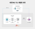
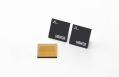
SK하이닉스가 네온 재활용 기술에 성공해, 네온 구입에 들어가는 비용과 온실가스 배출량을 줄이고, 네온 수급에 안정을 가져올 것으로 기대된다.
2024-04-01 오후 12:10:25by 배종인 기자

글로벌 제조 경기가 회복세를 보이면서 국내 수출입 및 주식시장에도 봄바람이 불고 있다.
2024-04-01 오후 5:00:56by 권신혁 기자
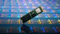
SK하이닉스가 미국 인디애나주(州) 웨스트라피엣(West Lafayette)에 AI 메모리용 어드밴스드 패키징 생산 기지를 건설하고, 퍼듀(Purdue) 대학교 등 현지 연구기관과 반도체 연구·개발에 협력하기로 했다.
2024-04-04 오전 8:55:12by 배종인 기자

SK하이닉스 P&T 담당 최우진 부사장은 지난 30년간 메모리 반도체 패키징 연구 개발에 매진하며, 최근 HBM으로 대표되는 AI 메모리의 핵심 기술로 부상한 이 분야를 이끌어 가고 있다.
2024-04-12 오전 11:31:34by 권신혁 기자

[열린보도원칙] 당 매체는 독자와 취재원 등 뉴스이용자의 권리 보장을 위해 반론이나 정정보도, 추후보도를 요청할 수 있는 창구를 열어두고 있음을 알려드립니다.
고충처리인 장은성 070-4699-5321 , news@e4ds.com