


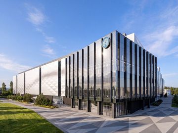
Applied Materials Unveils $5 Billion EPIC Center in Silicon Valley
Applied Materials has opened a $5 billion EPIC (Equipment, Process Innovation, and Commercialization) center in Silicon Valley. Major semiconductor ma…
2026.10.13 by 배종인 기자
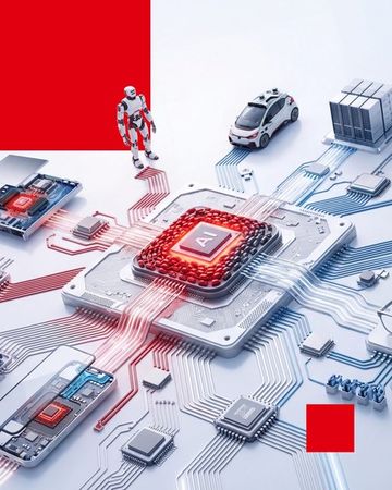
Henkel to Unveil Advanced Packaging Materials for AI and HBM at SEDEX 2026
Henkel will showcase semiconductor high-density packaging solutions for the AI and HBM era at SEDEX 2026. Through advanced materials such as underfill…
2026.10.06 by 배종인 기자
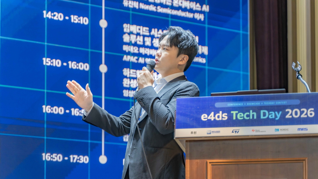

[e4ds Tech Day 2026 ⑥] Dong-Joo Shin, Mobilint CEO, "Winner of Physical AI Era is AI SoC, Not GPU"
At the keynote speech of 'e4ds Tech Day 2026', Dong-Joo Shin, CEO of Mobilint, stated that AI computation is shifting from GPU-centric to AI SoC and N…
2026.10.02 by 배종인 기자
Applied Materials and KIOXIA to Co-develop Next-Generation Memory at EPIC Center
Applied Materials and KIOXIA are undertaking joint development of next-generation memory for AI at the EPIC Center in Silicon Valley. The two companie…
2026.09.30 by 배종인 기자
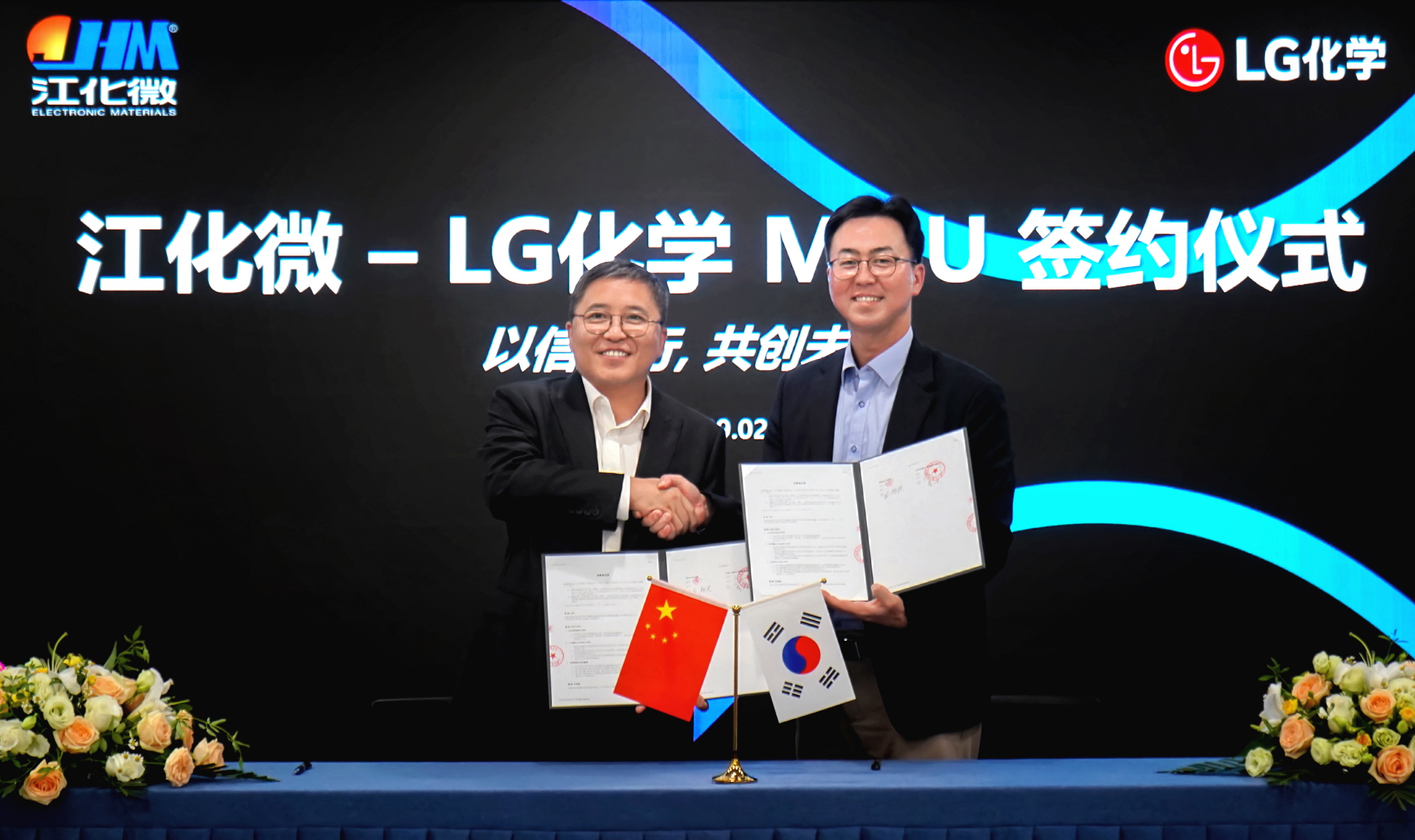
LG Chem Expands Semiconductor Cleaning Materials Business…Collaborates with China's Jianghua Wei on Ultra-high Purity IPA
LG Chem is moving to expand its ultra-high purity IPA (isopropyl alcohol) business, a core material for semiconductor processes. The company is buildi…
2026.09.14 by 배종인 기자
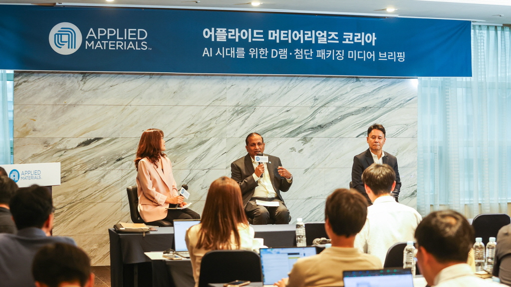
Applied Materials Targets 'Memory Wall' in AI Era...Presents Solutions Across D-RAM, HBM, and Packaging
In the artificial intelligence (AI) era, semiconductor industry competition hinges on 'data movement' rather than 'computation'. As AI models grow lar…
2026.08.31 by 배종인 기자
Semiconductor investment momentum shifts from front-end to back-end
The flow of semiconductor investment is shifting from front-end to back-end and packaging-focused processes. Global companies are concentrating on HBM…
2026.08.28 by 배종인 기자
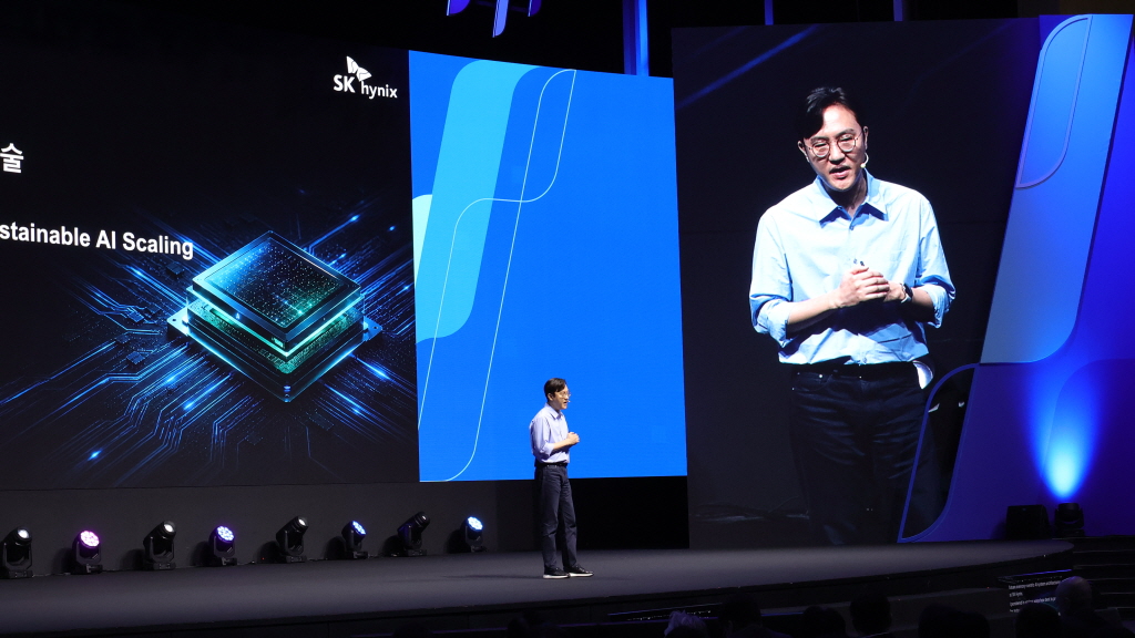
AI Agents Trigger 'Memory Supercycle'
At the 'Dell Technologies Forum 2026', SK Hynix Vice President Joo Young-pyo emphasized that as AI proliferation advances, memory bandwidth and effici…
2026.08.28 by 배종인 기자
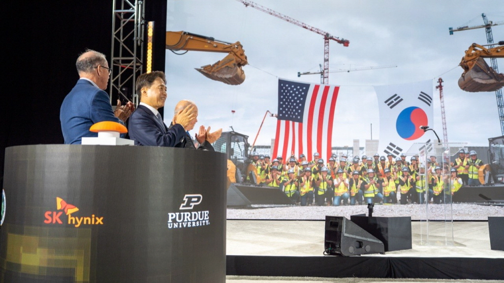
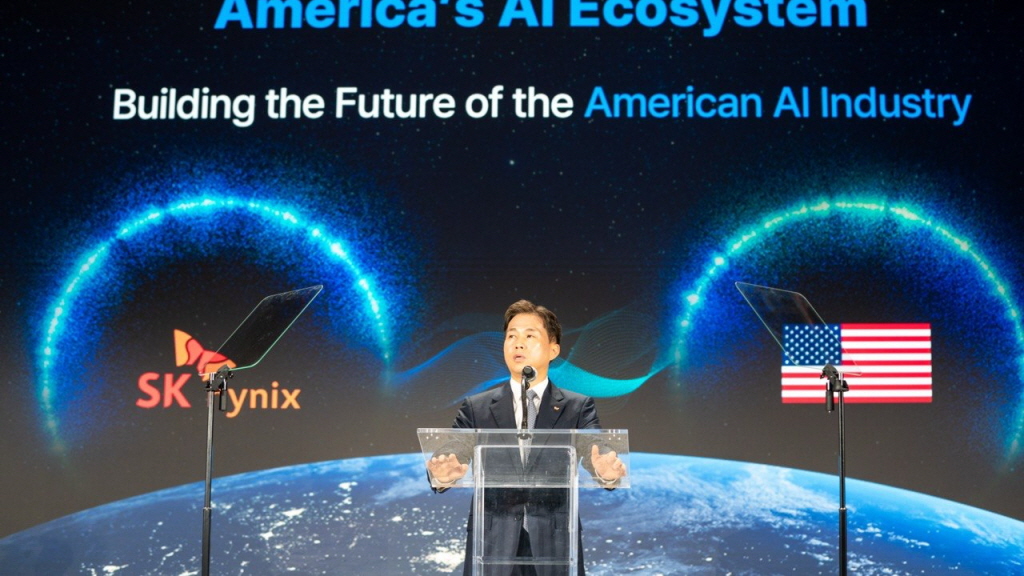
SK Hynix Breaks Ground on U.S. Indiana HBM Production Base...Mass Production of 'Made in USA' HBM in 2029
SK Hynix announced that it held a groundbreaking ceremony on the 27th (local time) for an advanced packaging production facility for AI memory in West…
2026.08.28 by 배종인 기자

Gartner "Memory Sales to Reach $837.3 Billion in 2026… 280% Year-over-Year Surge"
Gartner forecasts that the global semiconductor market will reach $1.5552 trillion in 2026. Expansion of AI infrastructure investment and memory price…
2026.08.25 by 명세환 기자
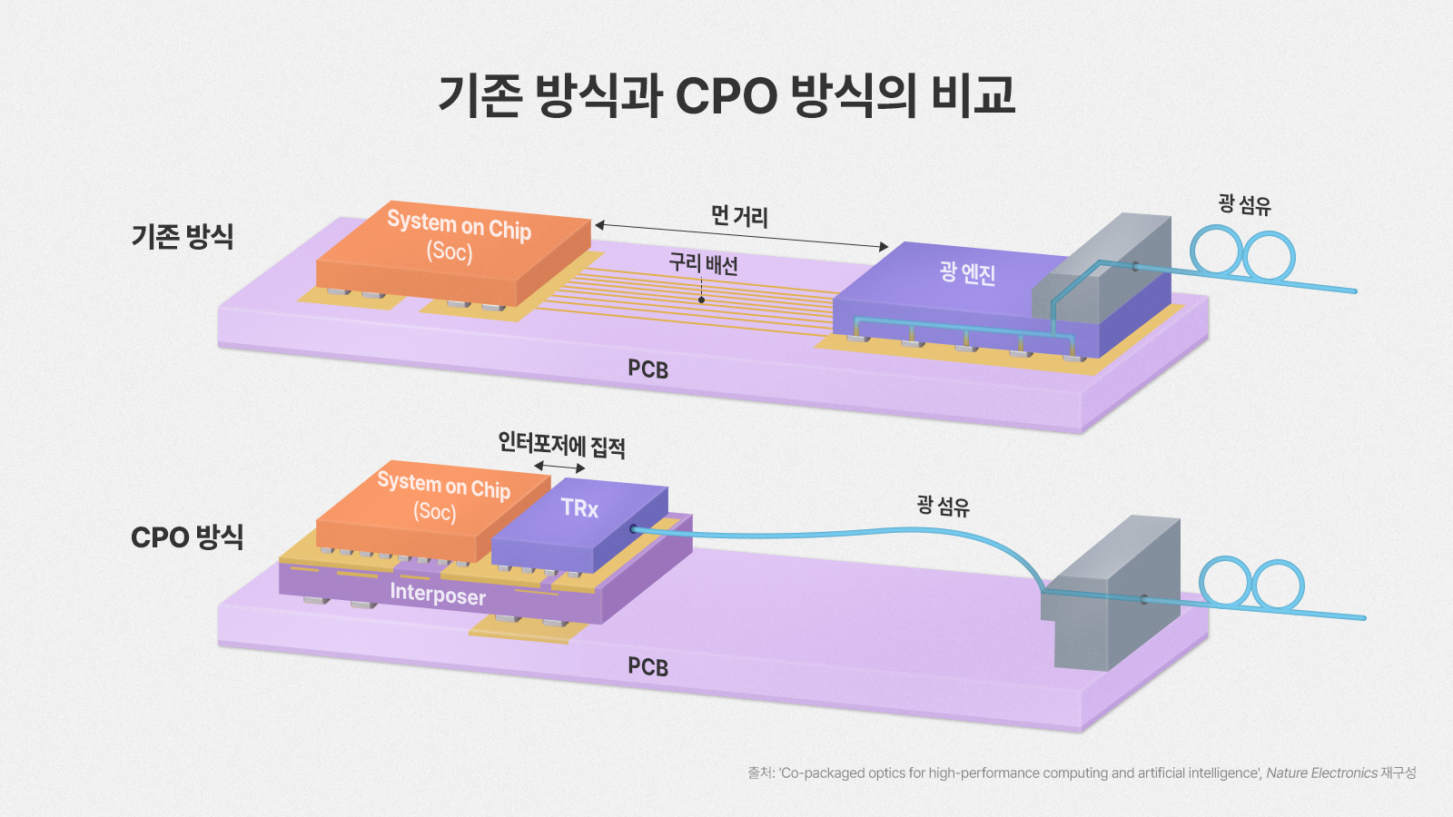
SK Hynix Unveils Next-Generation AI Infrastructure Blueprint Based on Optical Interconnect
SK Hynix has disclosed its CPO (Co-Packaged Optics) roadmap, a core technology for next-generation AI infrastructure, to Nature Electronics. To addres…
2026.08.21 by 배종인 기자
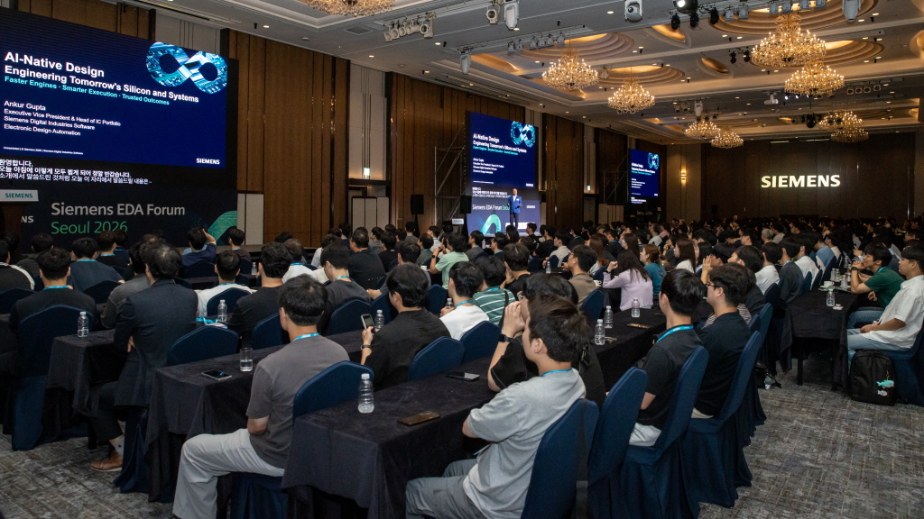
[EDA Great Transformation ③] Korea Was Already in the Midst of the EDA War
Competition among global EDA companies is intensifying in the Korean market, centered on Samsung's 2nm and HBM and 3D stacking. AI-based design automa…
2026.08.12 by 배종인 기자
SK Hynix Decides on 54 Trillion Won Investment in Yongin Y2 and Cheongju M17
SK Hynix will invest a total of 54 trillion won in Yongin and Cheongju to construct new semiconductor fabs in response to expanding AI demand. The Yon…
2026.08.10 by 배종인 기자
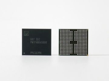
Samsung Electronics unveils zHBM and V10 BV-NAND mockups at FMS 2026
Samsung Electronics unveiled for the first time next-generation 3D memory architecture zHBM and V10 BV-NAND mockups at FMS 2026. zHBM features a struc…
2026.08.05 by 배종인 기자
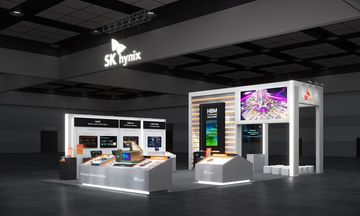
SK Hynix and SanDisk Unveil First HBF Standard Specification…Presenting AI Memory Strategy at FMS 2026
SK Hynix and SanDisk have unveiled the first standard specification for HBF (High Bandwidth Flash). Finalized within six months, this specification su…
2026.08.05 by 배종인 기자