기사입력 2024.08.01 11:32
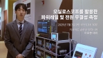
 램리서치가 양산성이 검증된 극저온 식각 기술을 통해 메모리 칩 제조사들이 목표로 하고 있는 2030년 1,000단 3D 낸드 양산을 실현하는데 적극 나선다.
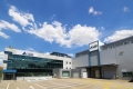
램리서치매뉴팩춰링코리아가 화성 공장 신설을 통해 국내 생산능력을 2배 높이고, 전세계 반도체 고객에 한발 앞서 지원한다.
2021-11-01 오후 4:30:20by 배종인 기자
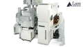
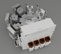
램리서치가 딥 실리콘 식각(Deep Silicon Etch) 기술을 확장해 300㎜ 웨이퍼에서도 소자를 생산할 수 새로운 식각 장비 출시로 자동차 및 스마트 기술용 칩 개발 지원에 본격 나선다.
2021-12-10 오후 3:08:11by 배종인 기자

웨이퍼 제조 장비 및 서비스를 공급하는 글로벌 반도체 장비 제조업체 램리서치(Lam Research Corporation)가 ‘세미콘 코리아 2022’에서 차세대 반도체 기술을 논의한다.
2022-02-07 오후 1:56:34by 배종인 기자
램리서치가 혁신적인 식각 기술 및 케미스트리 솔루션을 갖춘 고선택비 식각 장비 포트폴리오를 통해 첨단 로직 및 메모리 반도체 개발 솔루션 지원에 나선다.
2022-02-10 오후 5:38:24by 배종인 기자
.jpg)
이상원 현 램리서치코리아 대표이사가 램리서치매뉴팩춰링코리아 및 램리서치코리아테크놀로지 대표이사로 선임되며, 한국법인을 총괄한다.
2022-04-04 오후 1:46:36by 배종인 기자
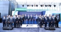
램리서치(Lam Research, CEO Tim Archer)가 코리아테크놀로지 센터를 통해 차세대 반도체 기술 혁신을 위한 고객과의 긴밀한 협력 및 솔루션 개발을 가속한다.
2022-04-26 오후 5:03:27by 배종인 기자
.jpg)
램리서치가 EUV 리소그래피용 건식(드라이) 포토레지스트 개발을 위해 인테그리스, 미쓰비시 케미칼 그룹 회사인 젤레스트와 손을 맞잡았다. 양산 성공시 세정작업이 없고, 소재 사용량도 적어 기존의 안정성 문제가 대두된 습식 레지스트를 대체할 수 있을 것으로 예상된다.
2022-07-20 오후 3:41:53by 배종인 기자

[열린보도원칙] 당 매체는 독자와 취재원 등 뉴스이용자의 권리 보장을 위해 반론이나 정정보도, 추후보도를 요청할 수 있는 창구를 열어두고 있음을 알려드립니다.
고충처리인 장은성 070-4699-5321 , news@e4ds.com