기사입력 2024.10.14 12:25

재료공학 솔루션 분야 글로벌 선도 기업 어플라이드 머티어리얼즈 코리아(대표 박광선)가 환경실천연합회와 업무협약(MOU)을 맺고 ‘우리 하천 지킴이 활동’을 4년 연속 후원, 지역사회 내 긍정적 영향력을 전파한다.
2024-03-08 오전 11:35:26by 배종인 기자

어플라이드 머티어리얼즈가 2024년도 인텔 협력사 부문에서 ‘EPIC(Excellence, Partnership, Inclusion and Continuous Improvement) 프로그램 우수 협력사 어워드’를 수상하며, 인텔의 글로벌 공급망에서 탁월함과 파트너십, 포용성, 지속적인 품질 개선에 대한 헌신에 대한 노력을 인정받았다.
2024-04-01 오후 1:37:25by 배종인 기자
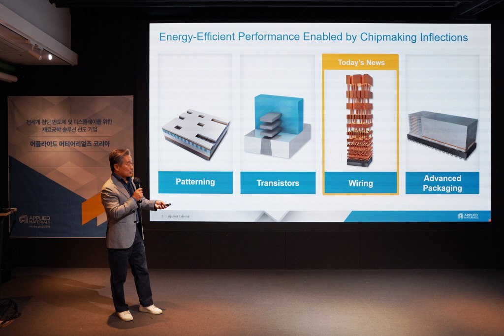
최근 첨단 반도체 파운드리 공정에서 1~2나노 차세대 기술 로드맵을 발표하며 초미세 패터닝에서 옹스트롬 시대가 열렸다. 인텔이 1.8나노에 해당하는 18옹스트롬 기반 로드맵을 본격화하는 가운데 이를 뒷받침하는 소재·장비사 기술 혁신 또한 발빠르게 기술 한계를 뛰어넘고 있다.
2024-04-04 오후 5:02:51by 권신혁 기자

재료공학 솔루션 분야 글로벌 선도 기업 어플라이드 머티어리얼즈가 5월12일부터 15일까지 서울 그랜드 워커힐 호텔에서 열리는 ‘국제 메모리 워크숍(IEEE IMW) 2024’에서 메모리 칩의 공정 장비 및 기술 발전에 대해 소개한다.
2024-05-07 오후 2:27:50by 배종인 기자
.jpg)
어플라이드 머티어리얼즈 회계연도 2024년 2분기 글로벌 매출은 미국 회계기준으로 66억5,000만달러, 매출총이익률 47.4%를 기록했다. 영업이익과 영업이익률은 각각 19억1,000만달러와 28.8%였으며, 주당순이익(EPS)은 2.06달러를 기록했다.
2024-05-17 오후 3:04:12by 배종인 기자

재료공학 솔루션 분야 글로벌 선도 기업 어플라이드 머티어리얼즈 코리아(대표 박광선)가 초록우산어린이재단과 지역사회 과학 문화 예술 교육을 위한 MOU를 체결하고, ‘어플라이드와 함께하는 과학교실’과 ‘어플라이드와 함께하는 전통문화교실’ 프로그램을 후원한다.
2024-06-24 오전 10:03:46by 배종인 기자
재료공학 솔루션 분야 글로벌 선도 기업 어플라이드 머티어리얼즈가 최근 발표한 ‘2023 지속가능성 보고서’에 따르면 미국 내 전력 소비량 100%, 전세계 전력 소비량의 70%를 신재생 에너지원으로 조달하는 등 탄소 배출량 감축에 있어 높은 성과를 보였다.
2024-07-01 오전 11:08:23by 배종인 기자
어플라이드 머티어리얼즈가 7월28일 마감한 회계연도 2024년 3분기 실적에서 AI 리더십 경쟁으로 인한 반도체 시장 호황에 예상을 뛰어넘는 호실적을 기록했다.
2024-08-21 오후 1:42:48by 배종인 기자

[열린보도원칙] 당 매체는 독자와 취재원 등 뉴스이용자의 권리 보장을 위해 반론이나 정정보도, 추후보도를 요청할 수 있는 창구를 열어두고 있음을 알려드립니다.
고충처리인 장은성 070-4699-5321 , news@e4ds.com