기사입력 2024.10.31 08:30
지능형 홈 로봇 분야의 글로벌 리더인 로보락은 인피니언 테크놀로지스(코리아 대표이사 이승수)의 REAL3™ ToF(Time-of-Flight)가 로보락의 지능형 청소 및 물걸레 올인원 로봇인 로보락 Qrevo Slim에 탑재되며, 컨슈머 로봇 시장에서 채용이 증가할 것으로 기대된다.
2024-09-10 오전 9:17:50by 배종인 기자
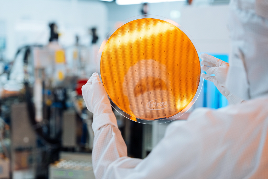
인피니언 테크놀로지스(코리아 대표이사 이승수)가 300㎜ 파워 GaN 웨이퍼 기술 개발에 성공하며, 200㎜ 웨이퍼 대비 더 많은 칩 생산으로 생산성과 효율성을 끌어올린다.
2024-09-12 오후 4:46:15by 배종인 기자

[편집자주] 자동차 산업의 메가 트렌드 가운데 차량의 편의성을 증대하는 다양한 기능 구현이 대세로 떠오르고 있다. 과거에는 없던 도어/트렁크 자동 개폐, 매립형 손잡이, 전동식 커튼, 전동 시트 및 진동 경고 스티어링 훨 등이 속속 등장하며 차량 내 모터 채택의 증가를 가속화하고 있다. 이에 여러 장치에 모터 제어 솔루션이 필요로 하게 되며 다양한 규격과 안전 기준을 충족하는 요구 또한 높아지게 됐다.
2024-09-20 오전 10:39:34by 권신혁 기자
최근 전기차·UAM·로봇을 비롯해 각종 산업 영역에서 모터 사용 비중이 증가하며, 정밀한 모터 제어 솔루션은 필수가 됐다. 이런 가운데 독일에 본사를 둔 MOTEON은 인피니언(Infineon) MOTIX™ 제품을 사용해 고성능 모터 제어를 위한 소프트웨어 솔루션을 제공하며, 산업 전반에 걸쳐 모터 제어의 신뢰성과 효율성을 향상 시키고 있다. 이에 본지는 10월31일 e4ds ee웨비나를 통해 MOTEON 모터제어 소프트웨어 솔루션을 소개하는 다보코퍼레이션(주) 기술연구소 조용규 연구소장과 만나 모터 정밀 제어에 대한 이야기를 들어봤다.
2024-10-15 오후 3:45:57by 배종인 기자
.jpg)
인피니언 테크놀로지스(코리아 대표이사 이승수)가 e-모빌리티 분야의 트랙션 인버터를 위한 새로운 HybridPACK™ Drive G2 Fusion 전력 모듈을 출시하며, 실리콘(Si)과 실리콘 카바이드(SiC)를 결합해 비용은 낮추고, 자동차의 성능과 효율은 높여 최적의 균형을 맞췄다.
2024-10-17 오후 4:27:16by 배종인 기자
인피니언 테크놀로지스(코리아 대표이사 이승수)가 자동차 애플리케이션의 식별 및 인증을 위한 동급 최고의 지문 센서 IC인 CYFP10020A00 및 CYFP10020S00을 출시하며, 자동차에서의 개인화 및 결제 애플리케이션 개발에 이상적인 솔루션을 제공한다.
2024-10-21 오전 11:21:43by 배종인 기자
인피니언 테크놀로지스(코리아 대표이사 이승수)의 자회사인 이미지몹(Imagimob)이 오토모티브 ASIL-D MCU인 인피니언의 AURIX™ TC3x 및 AURIX TC4x에 머신러닝 기능을 통합하며, 차량용 MCU도 자율주행 및 자동운전의 대량 데이터를 안전하고 실시간으로 처리할 수 있을 것으로 기대가 모아진다.
2024-10-29 오후 5:27:34by 배종인 기자

[열린보도원칙] 당 매체는 독자와 취재원 등 뉴스이용자의 권리 보장을 위해 반론이나 정정보도, 추후보도를 요청할 수 있는 창구를 열어두고 있음을 알려드립니다.
고충처리인 장은성 070-4699-5321 , news@e4ds.com


