기사입력 2024.11.18 14:31
삼성전자가 AI시대 초고용량 서버SSD를 위한 ‘1Tb(테라비트) QLC(Quad Level Cell) 9세대 V낸드’를 업계 최초로 양산했다.
2024-09-13 오전 10:17:43by 배종인 기자
.jpg)
삼성전자가 5나노 8세대 V낸드를 적용한 차량용 SSD를 출시하며, 업계 최고 속도로 고용량 파일에 빠르게 접근하며 자동차 메모리 시장에서 한 발 앞서나갔다.
2024-09-24 오전 8:36:26by 배종인 기자
이재용 삼성전자 회장이 지난 6일 필리핀 칼람바에 위치한 삼성전기 생산법인을 방문해 전기차, 자율주행사 확산으로 수요가 늘어나고 있는 MLCC 사업을 점검했다.
2024-10-07 오후 2:06:13by 배종인 기자
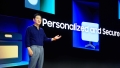
삼성전자가 3일 미국 새너제이 맥에너리 컨벤션 센터(San Jose McEnery Convention Center)에서 삼성 개발자 콘퍼런스(Samsung Developer Conference, 이하 SDC) 2024를 개최하고, 모바일, 가전 등 향후 개발 방향을 전제품군에 AI를 적용해 온디바이스 AI와 고성능 클라우드 AI를 결합하고 최적화하고 생성형 AI를 강화해 안전하고, 개인화된 경험을 제공하는 방향으로 나갈 것이라고 제시했다.
2024-10-07 오후 4:18:41by 배종인 기자
삼성전자가 2024년 3분기 기대치를 밑돈 실적에 이례적으로 반도체 수장이 직접 사과했다.
2024-10-09 오전 4:12:19by 배종인 기자
.jpg)
삼성전자가 AI PC 경험을 제공하는 '갤럭시 북5 Pro 360'을 28일 국내 출시한다. 갤럭시 북5 Pro 360은 인텔 코어 울트라 프로세서 시리즈 2(코드명 루나레이크)를 탑재한 Copilot+ PC로 AI 성능이 강조된다. AI 기능을 활용해 창작, 커뮤니케이션, 자료 검색 등을 보다 효율적으로 수행할 수 있다.
2024-10-16 오후 3:22:32by 권신혁 기자
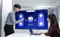
SK텔레콤(대표이사 CEO 유영상)과 삼성전자가 인공지능(AI)을 통해 5G 기지국 품질 최적화에 손을 맞잡으며, 기지국 성능이 극대화돼 소비자 체감 품질이 향상될 것으로 기대가 모아진다.
2024-10-28 오후 4:03:26by 배종인 기자

삼성전자가 2024년 3분기 분기 최대 매출을 기록했지만, 반도체 영업이익이 전월대비 반토막나며 웃지 못했다. 특히 경쟁사가 사상 최대의 영업이익을 기록한 다음에 이에 뒤처지는 부진한 실적에 시장의 실망감을 높였다.
2024-11-01 오후 4:17:52by 배종인 기자

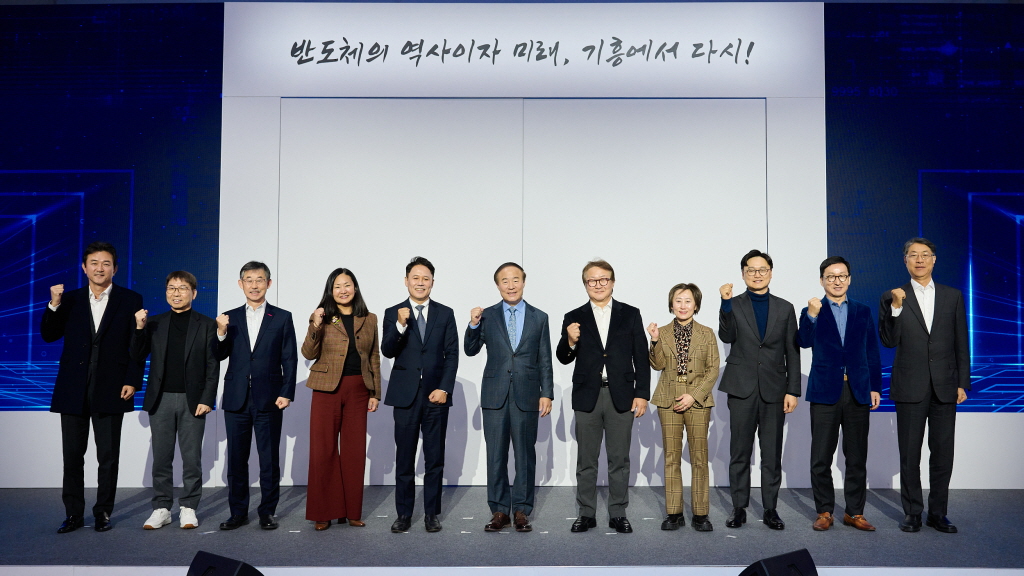
삼성전자가 수원컨벤션센터 및 삼성전자 서울 R&D 캠퍼스에서 삼성전자 SAIT(Samsung Advanced Institute of Technology) 주관으로 ‘삼성 AI 포럼 2024’를 개최하며 글로벌 AI 석학들과 AI의 미래에 대해 논의했다. 이 자리에서 한종희 삼성전자 대표이사 부회장은 AI를 더 책임감 있게 사용할 수 있을지가 갈수록 중요해진다며 삼성전자가 보다 효율적이고 지속 가능한 AI 생태계를 구축하는데 책임을 다할 것이라고 밝혔다.
2024-11-05 오전 10:00:44by 배종인 기자
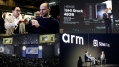
SK 그룹이 4일 ‘SK AI 서밋(SUMMIT) 2024’를, 삼성전자도 4일과 5일 ‘삼성 AI 포럼 2024’를, Arm도 1일 ‘Arm 테크 심포지아 2024’를 개최하는 등 11월 들어 주요 반도체 업체들이 AI 관련 대규모 행사를 개최하며, AI 시장 선점을 위한 주요 기술과 아젠다를 밝히고 있는 가운데, 더 이상 AI를 논하지 않고서는 반도체 시장에서 살아남을 수 없는 시대가 됐다.
2024-11-05 오전 11:44:28by 배종인 기자

[열린보도원칙] 당 매체는 독자와 취재원 등 뉴스이용자의 권리 보장을 위해 반론이나 정정보도, 추후보도를 요청할 수 있는 창구를 열어두고 있음을 알려드립니다.
고충처리인 장은성 070-4699-5321 , news@e4ds.com


