



ETRI develops gallium oxide MOSFET capable of withstanding 2300V high voltage.
 Published2019.05.19 10:02
| Implementing a robust semiconductor that can withstand high voltage and power
| 50% lower operating resistance and 25% higher breakdown voltage compared to existing products
In everyday life, laptops typically use adapters. While 220V power is supplied, laptop components struggle to withstand the voltage, requiring adapters to lower the voltage. Higher voltages are especially necessary for power-hungry devices like air conditioners, refrigerators, and vacuum cleaners.
If a material with high power conversion efficiency, such as gallium oxide, is used, the device will not heat up during operation, and less power will be wasted, saving energy. Gallium oxide (Ga2O3) is a semiconductor material, like silicon (Si), gallium nitride (GaN), and silicon carbide (SiC).
The Electronics and Telecommunications Research Institute (ETRI) announced on the 15th that it has developed the world's first power semiconductor transistor that can withstand high voltages of 2300V using gallium oxide. It is also called MOSFET.
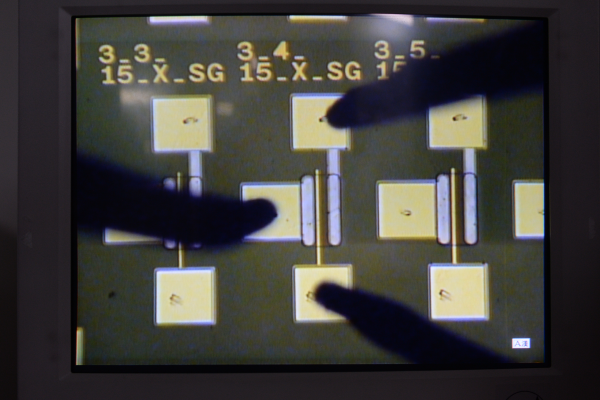
This technology is expected to be used in modules that convert power in electronic products, electric vehicles, wind power generation, locomotives, etc. that require high voltage, and thus it is expected to play a role as a strong semiconductor that can withstand high voltage and power.
Gallium oxide has a wider energy band gap than existing semiconductor materials, so it maintains semiconductor properties even at high temperatures and voltages, enabling chip miniaturization and high efficiency.
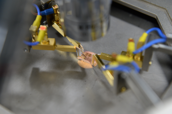
In addition, it is easy to make high-quality, large-area wafers from a solution, enabling the production of large, high-power devices at low cost, and is emerging as a next-generation power semiconductor device.
While existing power semiconductor devices were made by designing the device on silicon, gallium nitride, or silicon carbide and then going through patterning, etching, and deposition processes to create a transistor, the difference in this achievement is that it uses gallium oxide instead of existing semiconductors.
However, materials with wide band gaps, such as gallium oxide, have the disadvantage of low electrical conductivity. The research team revealed that the biggest challenge was to create a power semiconductor chip that could operate without losing its semiconductor properties even at high voltages and that allowed for good current flow.
To solve this difficult problem, the ETRI research team succeeded in breaking through the 2000V barrier for the first time by ▲designing channels and electrodes, which are the optimal path for electrons to pass through, ▲using semi-insulating substrates, and ▲adopting process and device structure design technologies. They developed a 2320V gallium oxide power semiconductor device technology that is at least 25% higher than the existing highest voltage level.
With this, a gallium oxide transistor was implemented that reduces the operating resistance by 50% and increases the breakdown voltage by 25% compared to the existing 1,850V power device of the University of Buffalo in the United States.
Currently, the gallium oxide power semiconductor device successfully developed by the research team measures 0.2 mm x 0.4 mm. If packaging is required to increase the chip size in the future, the current standard size is approximately 1.5 cm x 1.5 cm, but plans are in place to create a dedicated package to make it even smaller. The researchers said that the chip size can be made 30 to 50 percent smaller than that of current commercial products, allowing for two to three times more chip production per wafer.
In the future, this technology can be equally applied to large-area devices, and is expected to be widely used in new and renewable energy industries, including high-voltage direct current (HVDC) conversion equipment and solar and wind power generation.
Furthermore, the market outlook is bright as it can be utilized in a variety of industries, including next-generation automobiles such as electric vehicles, hydrogen vehicles, and autonomous vehicles, as well as home appliances such as refrigerators, washing machines, and air conditioners.
The research team plans to transfer the technology for the structure, device design, and manufacturing process of the newly developed transistor to power semiconductor chip manufacturers and power conversion module manufacturers.
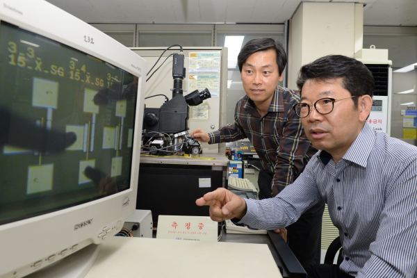
From left, Senior Researcher Jang Woo-jin and Senior Researcher Moon Jae-kyung
This research was conducted from 2017 as part of the project titled ‘Development of high-quality Ga2O3 epitaxial materials with low defects (<1x104cm-2) and power device technology with breakdown voltage of 1kV or higher’ of the Ministry of Trade, Industry and Energy and the Korea Evaluation Institute of Industrial Technology (KEIT).
The research team anticipates commercialization of this technology within five years, and has also published nine research papers and filed patent applications for related technologies for research and development of next-generation power devices.
Dr. Jae-kyung Moon of the ETRI RF/Power Components Research Group said, ““We plan to conduct additional research on the development of large-area, high-voltage, high-current devices with the goal of commercializing the world’s first gallium oxide power semiconductor,” he said.
Comments
Related news
.jpg)
ETRI Successfully Develops Nanocrystal Metamaterial Perfect Absorber: "Reflective Displays Now Sharper"
ETRI has successfully developed nanocrystalline-based broadband metamaterial perfect absorber technology. The research team fabricated a metamaterial perfect absorber in August of last year. However, absorption occurred only in a narrow band within the visible light wavelength range, making it difficult to achieve vivid reflected colors. The researchers resolved this issue by modifying the elements of the layers that comprise the metamaterial perfect absorber. The team formed layers using nanocrystalline metamaterial materials instead of conventional metals. As a result, they were able to increase optical loss and broaden the absorption bandwidth. While conventional metal-based absorbers had an absorption bandwidth of 28 nm, the nanocrystalline absorber extended up to 300 nm, more than 10 times greater, enabling the implementation of clearer reflected colors.
2019.04.24by 이수민 기자
ETRI, Develops 5G-WiFi-Wired Combination Technology… Accommodates 40 Times More Traffic Than LTE
The Electronics and Telecommunications Research Institute has successfully developed foundational technology enabling high-capacity internet services of up to 40Gbps by combining 5G, WiFi, and wired internet networks through joint research with domestic small and medium-sized enterprises including KT, Ranbird Technology, and S-NET ICT. The technology developed by the research team is a multi-access traffic aggregation technique that consolidates three networks into one. By controlling different wired and wireless access environments through a single 5G core network, it enables accommodation of traffic 40 times greater than 4G. With this technology, when simultaneously using 5G, WiFi, and wired internet networks, theoretically a maximum transmission speed of 40Gbps can be achieved by combining 5G's 20Gbps (which is up to 20 times faster than LTE), next-generation WiFi (802.11ax) maximum speed of 10Gbps, and wired internet at 10Gbps. In this case, immediate control of access network conditions is possible, allowing provision of an optimal access environment to users.
2019.05.12by 이수민 기자
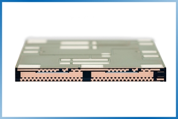
'Chip embedding technology' that embeds MOSFETs into PCBs improves performance of hybrid vehicle 48V systems
Infineon Technologies and Schweizer Electronics have developed new technology for mild hybrid vehicles. Chip embedding technology that integrates power MOSFETs into PCBs significantly improves the performance of 48V systems and reduces complexity. Continental Powertrain has decided to adopt this technology in 48V starter generators to be supplied to major European automotive manufacturers. The 48V starter generator is a key component that plays a crucial role in reducing CO2 emissions of mild hybrid vehicles by up to 15% compared to conventional drive trains.
2019.05.15by 이수민 기자

Intel Unveils Next-Generation 'Core Ultra Series 3' and vPro Platform for Enterprise PCs
Intel has officially unveiled the "Intel Core Ultra Series 3" for next-generation enterprise PCs and the latest vPro platform, addressing a wide range of demands from enterprise notebooks to high-performance workstations.
2026.03.26by 배종인 기자

ROHM Launches ESD Protection Diode Compatible with High-Speed Interfaces of 10Gbps or Higher
Semiconductor specialist ROHM has developed the 'RESDxVx series' of ESD (electrostatic discharge) protection diodes capable of responding to next-generation high-speed data communication environments exceeding 10Gbps, simultaneously enhancing both signal quality maintenance required in high-speed interfaces and IC protection performance.
2026.03.26by 배종인 기자











