


Spearhead of DRAM Speed Innovation, HBM2E Launched: "50% Faster than HBM2"
 Published2019.08.19 11:01
| Processing 460 GByte of data per second with 1,024 I/Os
16GB achieved by vertically connecting 8 16Gb chips via TSV
DRAM faster than HBM2, which is faster than DDR4, is being released.
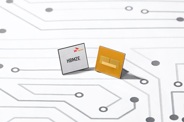
SK Hynix announced on the 12th that it has succeeded in developing HBM2E DRAM.
HBM2E is the next-generation product of HBM (High Bandwidth Memory) DRAM, which has a higher data processing speed than existing DRAM, and has increased the processing speed by 50% compared to the previous standard, HBM2.
Until a few years ago, memory bandwidth and system requirements increased proportionally.
However, recently, the demand for memory throughput across industries has surged due to advancements in AI, IoT, blockchain, RADAR, 5G, and 8K video. On the other hand, the increase in memory bandwidth has not been able to keep up with this.
Although the bandwidth of the most widely used DDR SDRAM has doubled with each generation over the past 20 years, the commercialization of DDR5 SDRAM is still a long way off in 2019. Furthermore, it seems difficult to keep up with recent trends with only a twofold increase in bandwidth.
HBM2E developed by SK Hynix can achieve a processing speed of 3.6 gigabits (Gbit/s), enabling 460 gigabytes (GByte) of data processing per second through 1,024 I/Os.
This is a level capable of processing data equivalent to 124 FHD (Full-HD) movies (3.7GB) in one second.
The capacity is 16GB, achieved by vertically connecting eight 16Gb chips using TSV (Through Silicon Via) technology on a single product basis.
TSV is an interconnection technology that drills thousands of tiny holes in a DRAM chip and connects the holes of the upper and lower chips with electrodes that penetrate vertically.
HBM2E is a high-specification memory solution suitable for systems based on the Fourth Industrial Revolution, such as machine learning, supercomputers, and AI, as well as high-performance GPUs that require ultra-high speed characteristics.
HBM does not use the conventional method of creating memory chips in the form of modules and connecting them to the motherboard; instead, the chips themselves are mounted close to logic chips such as GPUs at a distance of tens of micrometers (µm). SK Hynix announced the first-generation HBM product with AMD in 2013 and developed HBM2 with Samsung Electronics in 2016.
"SK Hynix HBM Business Strategy Manager Jun-Hyeon Jeon stated, 'SK Hynix will begin full-scale mass production starting in 2020 when the HBM2E market opens, and will continue to strengthen its leadership in the premium memory market.'"
Comments 1
1 Comments:
Related news
Low-power, miniaturized HBM2 that controls large-capacity memory
With the development of AI, IoT, blockchain, RADAR, 5G, and 8K video, memory throughput is surging rapidly. However, existing memory bandwidth is unable to keep pace with the increasing system requirements. The industry is seeking high-capacity memory solutions through HBM2 DRAM utilizing TSV technology.
2018.08.28by 이수민 기자
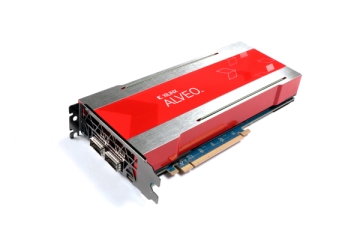
Xilinx Launches Alveo U280 with HBM2 for Data Center Acceleration
Xilinx announced the expansion of its product line by adding the latest Alveo U280 product to its Alveo data center accelerator card portfolio. The Alveo U280 card supports advanced high-performance server interconnects including HBM2. The Alveo portfolio is designed to enhance the performance of industry-standard servers in cloud and on-premises data centers.
2018.11.15by 이수민 기자
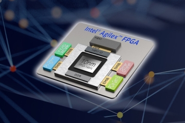
The surge in IDC traffic in the 5G era… FPGAs are the answer.
The importance of data centers and the utilization rate of IoT devices have increased significantly in recent years. Consequently, the demand for FPGAs is gradually rising in various application fields that previously relied mainly on conventional processors. This is because FPGAs offer better efficiency than traditional processors for specialized purposes. Agilex, the first FPGA released by Intel following its acquisition of Altera, has drawn attention as a semiconductor manufactured using Intel's 10nm process. An even more interesting aspect is that it supports CXL specifications, a recently disclosed next-generation interface standard, as well as PCIe 5.0. Agilex can secure sufficient bandwidth even when used alongside dedicated accelerators such as CPUs and GPUs. Moreover, it not only supports ultra-high-speed memory such as DDR5 and HBM2, but also supports Intel Optane DC Persistent Memory.
2019.06.03by 이수민 기자

Intel Unveils Next-Generation 'Core Ultra Series 3' and vPro Platform for Enterprise PCs
Intel has officially unveiled the "Intel Core Ultra Series 3" for next-generation enterprise PCs and the latest vPro platform, addressing a wide range of demands from enterprise notebooks to high-performance workstations.
2026.03.26by 배종인 기자

ROHM Launches ESD Protection Diode Compatible with High-Speed Interfaces of 10Gbps or Higher
Semiconductor specialist ROHM has developed the 'RESDxVx series' of ESD (electrostatic discharge) protection diodes capable of responding to next-generation high-speed data communication environments exceeding 10Gbps, simultaneously enhancing both signal quality maintenance required in high-speed interfaces and IC protection performance.
2026.03.26by 배종인 기자












좋은 정보 감사합니다